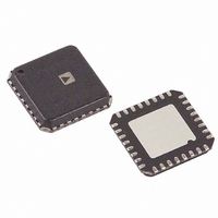
ADF4193BCPZ Analog Devices Inc, ADF4193BCPZ Datasheet - Page 7

ADF4193BCPZ
Manufacturer Part Number
ADF4193BCPZ
Description
IC PLL FREQ SYNTHESIZER 32LFCSP
Manufacturer
Analog Devices Inc
Type
Clock/Frequency Synthesizer (RF)r
Datasheet
1.ADF4193BCPZ.pdf
(28 pages)
Specifications of ADF4193BCPZ
Pll
Yes
Input
CMOS
Output
Clock
Number Of Circuits
1
Ratio - Input:output
2:1
Differential - Input:output
Yes/No
Frequency - Max
3.5GHz
Divider/multiplier
Yes/Yes
Voltage - Supply
2.7 V ~ 3.3 V
Operating Temperature
-40°C ~ 85°C
Mounting Type
Surface Mount
Package / Case
32-LFCSP
Frequency-max
3.5GHz
Pll Type
Frequency Synthesis
Frequency
3.5GHz
Supply Current
24mA
Supply Voltage Range
2.7V To 3.3V
Digital Ic Case Style
LFCSP
No. Of Pins
32
Operating Temperature Range
-40°C To +85°C
Lead Free Status / RoHS Status
Lead free / RoHS Compliant
For Use With
EVAL-ADF4193EBZ2 - BOARD EVALUATION EB2 FOR ADF4193EVAL-ADF4193EBZ1 - BOARD EVALUATION EB1 FOR ADF4193
Lead Free Status / RoHS Status
Lead free / RoHS Compliant, Lead free / RoHS Compliant
Available stocks
Company
Part Number
Manufacturer
Quantity
Price
Part Number:
ADF4193BCPZ
Manufacturer:
ADI/亚德诺
Quantity:
20 000
Company:
Part Number:
ADF4193BCPZ-RL7
Manufacturer:
AD
Quantity:
800
Part Number:
ADF4193BCPZ-RL7
Manufacturer:
ADI/亚德诺
Quantity:
20 000
Pin No.
23
24
25
26
27
28
29
30
31
32
R
V
AIN−
CP
SW2
SW
SW1
CP
AIN+
V
Mnemonic
SET
P
P
2
3
OUT−
OUT+
GND
Description
Connecting a resistor between this pin and GND sets the charge pump output current. The nominal voltage bias at
the R
So, with R
Power Supply Pin for the Charge Pump. Nominally 5 V, should be at the same voltage at V
capacitor to ground should be placed as close as possible to this pin.
Differential Amplifier’s Negative Input Pin.
Differential Charge Pump’s Negative Output Pin. Should be connected to AIN− and the loop filter.
Fast Lock Switch 2. This switch is closed to SW
Common for SW1 and SW2 Switches. Should be connected to the ground plane.
Fast Lock Switch 1. This switch is closed to SW
Differential Charge Pump’s Positive Output Pin. Should be connected to AIN+ and the loop filter.
Differential Amplifier’s Positive Input Pin.
Power Supply Pin for the Differential Amplifier. This can range from 5.0 V to 5.5 V. A 0.1 μF decoupling capacitor to
ground should be placed as close as possible to this pin. Also requires a 10 μF decoupling capacitor to ground.
I
SET
CP
pin is 0.55 V. The relationship between I
= 0.25/R
SET
= 2.4 kΩ, I
SET
CP
= 104 μA.
Rev. C | Page 7 of 28
GND
GND
CP
while the SW1/SW2 timeout counter is active.
while the SW1/SW2 timeout counter is active.
and R
SET
is
P
1. A 0.1 μF decoupling
ADF4193


