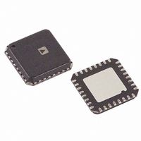
ADF4193BCPZ Analog Devices Inc, ADF4193BCPZ Datasheet - Page 16

ADF4193BCPZ
Manufacturer Part Number
ADF4193BCPZ
Description
IC PLL FREQ SYNTHESIZER 32LFCSP
Manufacturer
Analog Devices Inc
Type
Clock/Frequency Synthesizer (RF)r
Datasheet
1.ADF4193BCPZ.pdf
(28 pages)
Specifications of ADF4193BCPZ
Pll
Yes
Input
CMOS
Output
Clock
Number Of Circuits
1
Ratio - Input:output
2:1
Differential - Input:output
Yes/No
Frequency - Max
3.5GHz
Divider/multiplier
Yes/Yes
Voltage - Supply
2.7 V ~ 3.3 V
Operating Temperature
-40°C ~ 85°C
Mounting Type
Surface Mount
Package / Case
32-LFCSP
Frequency-max
3.5GHz
Pll Type
Frequency Synthesis
Frequency
3.5GHz
Supply Current
24mA
Supply Voltage Range
2.7V To 3.3V
Digital Ic Case Style
LFCSP
No. Of Pins
32
Operating Temperature Range
-40°C To +85°C
Lead Free Status / RoHS Status
Lead free / RoHS Compliant
For Use With
EVAL-ADF4193EBZ2 - BOARD EVALUATION EB2 FOR ADF4193EVAL-ADF4193EBZ1 - BOARD EVALUATION EB1 FOR ADF4193
Lead Free Status / RoHS Status
Lead free / RoHS Compliant, Lead free / RoHS Compliant
Available stocks
Company
Part Number
Manufacturer
Quantity
Price
Part Number:
ADF4193BCPZ
Manufacturer:
ADI/亚德诺
Quantity:
20 000
Company:
Part Number:
ADF4193BCPZ-RL7
Manufacturer:
AD
Quantity:
800
Part Number:
ADF4193BCPZ-RL7
Manufacturer:
ADI/亚德诺
Quantity:
20 000
ADF4193
MOD/R REGISTER (R1)
This register is used to set the PFD reference frequency and the
channel step size, which is determined by the PFD frequency
divided by the fractional modulus. Note that the MOD, R
counter, REF/2, CP ADJ, and doubler enable bits are double
buffered. They do not take effect until the next write to R0
(FRAC/INT register) is complete.
Control Bits
With C3, C2, and C1 set to 0, 0, 1, respectively, the MOD/R
register (R1) is programmed.
CP ADJ
When this bit is set to 1, the charge pump current is scaled up
25% from its nominal value on the next write to R0. When this
bit is set to 0, the charge pump current stays at its nominal value
on the next write to R0. See the Programming section for more
information on how this feature can be used.
REF/2
Setting this bit to 1 inserts a divide-by-2, toggle flip-flop between
the R counter and PFD, which extends the maximum REF
input rate.
DB23
F5
0
1
F5
F4
0
1
CP ADJ
NOMINAL
ADJUSTED
DB22
REF/2
DISABLE
ENABLE
F4
F2
0
1
PRESCALER
4/5
8/9
DB21
0
DB20
F2
DB19
F1
F1
0
1
DOUBLER ENABLE
DOUBLER DISABLED
DOUBLER ENABLED
DB18
R4
DB17
R COUNTER
R3
4-BIT RF
DB16
R4
0
0
0
0
.
.
.
1
1
1
1
R2
DB15
R3
0
0
0
1
.
.
.
1
1
1
1
R1
DB14
M12
M12
0
0
0
.
.
.
1
1
1
1
R2
0
1
1
0
.
.
.
0
0
1
1
Figure 30. MOD/R Register (R1)
IN
DB13
M11
Rev. C | Page 16 of 28
M11
0
0
0
.
.
.
1
1
1
1
R1
1
0
1
0
.
.
.
0
1
0
1
DB12
M10
M10
0
0
0
.
.
.
1
1
1
1
RF R COUNTER DIVIDE RATIO
1
2
3
4
.
.
.
12
13
14
15
DB11
M9
..........
..........
..........
..........
..........
..........
..........
..........
..........
..........
Reserved Bit
Reserved Bit DB21 must be set to 0.
Doubler Enable
Setting this bit to 1 inserts a frequency doubler between REF
and the 4-bit R counter. Setting this bit to 0 bypasses the doubler.
4-Bit RF R Counter
It allows the REF
reference clock to the PFD. All integer values from 1 to 15 are
allowed. See the Worked Example section.
12-Bit Interpolator Modulus
For a given PFD reference frequency, the fractional deno-
minator or modulus sets the channel step resolution at the
RF output. All integer values from 13 to 4095 are allowed.
See the Programming section for additional information and
guidelines for selecting the value of MOD.
DB10
M8
12-BIT MODULUS
M3
1
1
1
.
.
.
1
1
1
1
DB9
M7
DB8
M2
0
1
1
.
.
.
0
0
1
1
M6
IN
frequency to be divided down to produce the
DB7
M5
M1
1
0
1
.
.
.
0
1
0
1
DB6
M4
INTERPOLATOR MODULUS VALUE (MOD)
13
14
15
.
.
.
4092
4093
4094
4095
DB5
M3
DB4
M2
DB3
M1
C3 (0)
DB2
CONTROL
C2 (0)
BITS
DB1
C1 (1)
DB0
IN


