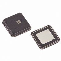
ADF4193BCPZ Analog Devices Inc, ADF4193BCPZ Datasheet - Page 11

ADF4193BCPZ
Manufacturer Part Number
ADF4193BCPZ
Description
IC PLL FREQ SYNTHESIZER 32LFCSP
Manufacturer
Analog Devices Inc
Type
Clock/Frequency Synthesizer (RF)r
Datasheet
1.ADF4193BCPZ.pdf
(28 pages)
Specifications of ADF4193BCPZ
Pll
Yes
Input
CMOS
Output
Clock
Number Of Circuits
1
Ratio - Input:output
2:1
Differential - Input:output
Yes/No
Frequency - Max
3.5GHz
Divider/multiplier
Yes/Yes
Voltage - Supply
2.7 V ~ 3.3 V
Operating Temperature
-40°C ~ 85°C
Mounting Type
Surface Mount
Package / Case
32-LFCSP
Frequency-max
3.5GHz
Pll Type
Frequency Synthesis
Frequency
3.5GHz
Supply Current
24mA
Supply Voltage Range
2.7V To 3.3V
Digital Ic Case Style
LFCSP
No. Of Pins
32
Operating Temperature Range
-40°C To +85°C
Lead Free Status / RoHS Status
Lead free / RoHS Compliant
For Use With
EVAL-ADF4193EBZ2 - BOARD EVALUATION EB2 FOR ADF4193EVAL-ADF4193EBZ1 - BOARD EVALUATION EB1 FOR ADF4193
Lead Free Status / RoHS Status
Lead free / RoHS Compliant, Lead free / RoHS Compliant
Available stocks
Company
Part Number
Manufacturer
Quantity
Price
Part Number:
ADF4193BCPZ
Manufacturer:
ADI/亚德诺
Quantity:
20 000
Company:
Part Number:
ADF4193BCPZ-RL7
Manufacturer:
AD
Quantity:
800
Part Number:
ADF4193BCPZ-RL7
Manufacturer:
ADI/亚德诺
Quantity:
20 000
THEORY OF OPERATION
The ADF4193 is targeted at GSM base station requirements,
specifically to eliminate the need for ping-pong solutions. It
works based on fast lock, using a wide loop bandwidth during a
frequency change and narrowing the loop bandwidth once
frequency lock is achieved. Widening the loop bandwidth is
achieved by increasing the charge pump current. Switches are
included to change the loop filter component values to maintain
stability with the changing charge pump current. The narrow
loop bandwidth ensures that phase noise and spur specifications
are met. A differential charge pump and loop filter topology are
used to ensure that the fast lock time benefit from widening the
loop bandwidth is maintained when the loop is restored to
narrow bandwidth mode for normal operation.
REFERENCE INPUT SECTION
The reference input stage is shown in Figure 20. Switches S1 and
S2 are normally closed, and S3 is normally open. During power-
down, S3 is closed, and S1 and S2 are opened to ensure that
there is no loading of the REF
the active edge at the positive edge triggered PFD.
R Counter and Doubler
The 4-bit R counter allows the input reference frequency to be
divided down to produce the reference clock to the phase
frequency detector (PFD). A toggle flip-flop can be optionally
inserted after the R counter to give a further divide-by-2. Using
this option has the additional advantage of ensuring that the
PFD reference clock has a 50/50 mark-space ratio. This ratio
gives the maximum separation between the fast lock timer
clock, which is generated off the falling edge of the PFD
reference, and the rising edge, which is the active edge in the
PFD. It is recommended that this toggle flip-flop be enabled for
all even R divide values greater than 2. It must be enabled if
dividing down a REF
An optional doubler before the 4-bit R counter can be used for
low REF
options, reference division ratios from 0.5 to 30 between REF
and the PFD are possible.
IN
frequencies, up to 20 MHz. With these programmable
REF
IN
NC
Figure 20. Reference Input Stage
POWER-DOWN
S1
CONTROL
IN
NO
frequency that is greater than 120 MHz.
NC
S3
S2
IN
100kΩ
pin. The falling edge of REF
BUFFER
TO R COUNTER
IN
Rev. C | Page 11 of 28
IN
is
RF INPUT STAGE
The RF input stage is shown in Figure 21. It is followed by a
2-stage limiting amplifier to generate the CML clock levels
needed for the prescaler. Two prescaler options are selectable: a
4/5 and an 8/9. The 8/9 prescaler is selected for N divider values
greater than 80.
RF N Divider
The RF N divider allows a fractional division ratio in the PLL
feedback path. The integer and fractional parts of the division
are programmed using separate registers, as shown in Figure 22
and described in the INT, FRAC, and MOD Relationship
section. Integer division ratios from 26 to 255 are allowed and a
third-order, Σ-Δ modulator interpolates the fractional value
between the integer steps.
INT, FRAC, and MOD Relationship
The INT, FRAC, and MOD values, programmed through the
serial interface, make it possible to generate RF output frequencies
that are spaced by fractions of the PFD reference frequency.
The N divider value, shown inside the brackets of the following
equation for the RF VCO frequency (RF
integer part (INT) and a fractional part (FRAC/MOD):
where:
RF
F
PFD
OUT
INPUT STAGE
is the PFD reference frequency.
FROM RF
RF
is the output frequency of the external VCO.
RF
RF
OUT
IN+
IN–
= F
PFD
GENERATOR
RF N DIVIDER
N COUNTER
× [INT + (FRAC/MOD)]
BIAS
Figure 22. Fractional-N Divider
REG
INT
Figure 21. RF Input Stage
500Ω
1.6V
MOD
REG
N = INT + FRAC/MOD
INTERPOLATOR
500Ω
THIRD-ORDER
FRACTIONAL
OUT
), is made up of an
VALUE
FRAC
AGND
AV
DD
ADF4193
TO PFD


