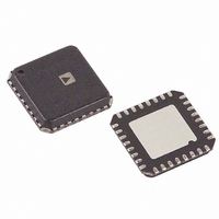
ADF4193BCPZ Analog Devices Inc, ADF4193BCPZ Datasheet - Page 4

ADF4193BCPZ
Manufacturer Part Number
ADF4193BCPZ
Description
IC PLL FREQ SYNTHESIZER 32LFCSP
Manufacturer
Analog Devices Inc
Type
Clock/Frequency Synthesizer (RF)r
Datasheet
1.ADF4193BCPZ.pdf
(28 pages)
Specifications of ADF4193BCPZ
Pll
Yes
Input
CMOS
Output
Clock
Number Of Circuits
1
Ratio - Input:output
2:1
Differential - Input:output
Yes/No
Frequency - Max
3.5GHz
Divider/multiplier
Yes/Yes
Voltage - Supply
2.7 V ~ 3.3 V
Operating Temperature
-40°C ~ 85°C
Mounting Type
Surface Mount
Package / Case
32-LFCSP
Frequency-max
3.5GHz
Pll Type
Frequency Synthesis
Frequency
3.5GHz
Supply Current
24mA
Supply Voltage Range
2.7V To 3.3V
Digital Ic Case Style
LFCSP
No. Of Pins
32
Operating Temperature Range
-40°C To +85°C
Lead Free Status / RoHS Status
Lead free / RoHS Compliant
For Use With
EVAL-ADF4193EBZ2 - BOARD EVALUATION EB2 FOR ADF4193EVAL-ADF4193EBZ1 - BOARD EVALUATION EB1 FOR ADF4193
Lead Free Status / RoHS Status
Lead free / RoHS Compliant, Lead free / RoHS Compliant
Available stocks
Company
Part Number
Manufacturer
Quantity
Price
Part Number:
ADF4193BCPZ
Manufacturer:
ADI/亚德诺
Quantity:
20 000
Company:
Part Number:
ADF4193BCPZ-RL7
Manufacturer:
AD
Quantity:
800
Part Number:
ADF4193BCPZ-RL7
Manufacturer:
ADI/亚德诺
Quantity:
20 000
ADF4193
Parameter
SW1, SW2, and SW3
NOISE CHARACTERISTICS
1
2
3
4
5
6
TIMING CHARACTERISTICS
AV
50 Ω, T
Table 2.
Parameter
t
t
t
t
t
t
t
1
2
1
2
3
4
5
6
7
Operating temperature range is from −40°C to +85°C.
Operating temperature range is from −40°C to +105°C
The prescaler value is chosen to ensure that the RF input is divided down to a frequency that is less than this value.
f
f
Calculated from the phase noise measured at 5 kHz with a 60 kHz loop BW. Increased noise contribution from the differential amplifier if the loop BW is reduced.
Operating temperature is from −40°C to +85°C.
Operating temperature is from −40°C to +105°C.
REFIN
REFIN
I
I
I
R
R
900 MHz Output
1800 MHz Output
Phase Noise Figure of Merit
DD
DD
DD
DD
ON
ON
= 26 MHz; f
= 13 MHz; f
(V
(V
Power-Down
= DV
(SW1 and SW2)
SW3
P
P
A
1 + V
3)
= T
DATA
DD
CLK
MIN
P
LE
LE
2)
STEP
STEP
= 3 V ± 10%, V
to T
= 200 kHz; f
= 200 kHz; f
4
5
MAX
Limit (B Version)
10
10
10
15
15
10
15
, unless otherwise noted.
RF
RF
(MSB)
DB23
= 900 MHz; loop BW = 40 kHz.
= 1850 MHz; loop BW = 60 kHz.
t
6
P
1
1, V
P
2 = 5 V ± 10%, V
1
B Version
27
30
10
65
75
−108
−102
−216
t
2
DB22
1
t
3
Limit (C Version)
10
10
10
15
15
10
15
P
3 = 5.35 V ± 5%, AGND = DGND = GND = 0 V, R
Figure 2. Timing Diagram
Rev. C | Page 4 of 28
C Version
30
35
10
65
75
−108
−102
−216
DB2
t
4
2
2
t
5
(CONTROL BIT C2)
Unit
ns min
ns min
ns min
ns min
ns min
ns min
ns min
Unit
mA max
mA max
μA typ
Ω typ
Ω typ
dBc/Hz typ
dBc/Hz typ
dBc/Hz typ
DB1
Test Conditions/Comments
LE setup time
DATA to CLOCK setup time
DATA to CLOCK hold time
CLOCK high duration
CLOCK low duration
CLOCK to LE setup time
LE pulse width
Test Conditions/Comments
22 mA typ
24 mA typ
@ 5 kHz offset and 26 MHz PFD
frequency
@ 5 kHz offset and 13 MHz PFD
frequency
@ VCO output with dither off
(CONTROL BIT C1)
SET
DB0 (LSB)
= 2.4 kΩ, dBm referred to
t
t
6
7


