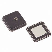
ADF4193BCPZ Analog Devices Inc, ADF4193BCPZ Datasheet - Page 19

ADF4193BCPZ
Manufacturer Part Number
ADF4193BCPZ
Description
IC PLL FREQ SYNTHESIZER 32LFCSP
Manufacturer
Analog Devices Inc
Type
Clock/Frequency Synthesizer (RF)r
Datasheet
1.ADF4193BCPZ.pdf
(28 pages)
Specifications of ADF4193BCPZ
Pll
Yes
Input
CMOS
Output
Clock
Number Of Circuits
1
Ratio - Input:output
2:1
Differential - Input:output
Yes/No
Frequency - Max
3.5GHz
Divider/multiplier
Yes/Yes
Voltage - Supply
2.7 V ~ 3.3 V
Operating Temperature
-40°C ~ 85°C
Mounting Type
Surface Mount
Package / Case
32-LFCSP
Frequency-max
3.5GHz
Pll Type
Frequency Synthesis
Frequency
3.5GHz
Supply Current
24mA
Supply Voltage Range
2.7V To 3.3V
Digital Ic Case Style
LFCSP
No. Of Pins
32
Operating Temperature Range
-40°C To +85°C
Lead Free Status / RoHS Status
Lead free / RoHS Compliant
For Use With
EVAL-ADF4193EBZ2 - BOARD EVALUATION EB2 FOR ADF4193EVAL-ADF4193EBZ1 - BOARD EVALUATION EB1 FOR ADF4193
Lead Free Status / RoHS Status
Lead free / RoHS Compliant, Lead free / RoHS Compliant
Available stocks
Company
Part Number
Manufacturer
Quantity
Price
Part Number:
ADF4193BCPZ
Manufacturer:
ADI/亚德诺
Quantity:
20 000
Company:
Part Number:
ADF4193BCPZ-RL7
Manufacturer:
AD
Quantity:
800
Part Number:
ADF4193BCPZ-RL7
Manufacturer:
ADI/亚德诺
Quantity:
20 000
CHARGE PUMP REGISTER (R4)
Reserved Bits
Bit DB23 to Bit DB14 are reserved and should be set to hex
code 001 for normal operation.
9-Bit Timeout Counter
These bits are used to program the fast lock timeout counters.
The counters are clocked at one-quarter the PFD reference
frequency, therefore, their time delay scales with the PFD
frequency according to
For example, if 35 were loaded with timer select (00) with a
13 MHz PFD, then SW1/SW2 would be switched after
Timer Select
These two address bits select the timeout counter to be
programmed. Note that to set up the ADF4193 correctly
requires setup of these three timeout counters; therefore, three
writes to this register are required in the initialization sequence.
Table 6 shows example values for a GSM Tx synthesizer with a
60 kHz final loop BW. See the Applications section for more
information.
DB23
0
Delay(s) = (Timeout Counter Value × 4)/(PFD Frequency)
(35 × 4)/13 MHz = 10.8 μs
DB22
0
DB21
0
DB20
0
DB19
RESERVED
0
DB18
0
DB17
0
DB16
0
DB15
0
C9
0
0
0
0
.
.
.
1
1
1
1
DB14
1
Figure 33. Charge Pump Register (R4)
C8
0
0
0
0
.
.
.
1
1
1
1
DB13
C9
Rev. C | Page 19 of 28
C7
0
0
0
0
.
.
.
1
1
1
1
DB12
C8
..........
..........
..........
..........
..........
..........
..........
..........
..........
..........
..........
DB11
C7
9-BIT TIMEOUT COUNTER
Table 6. Recommended Values for a GSM Tx LO
Timer Select
10
01
00
On each write to R0, the timeout counters start. Switch SW3
closes until the SW3 counter times out. Similarly, switches
SW1/SW2 close until the SW1/SW2 counter times out. When
the ICP counter times out, the charge pump current is ramped
down from 64× to 1× in six binary steps. It is recommended
that the SW1, SW2, and SW3 timeout counter values are set
equal to the ICP timeout counter value plus 7, as in the example
of Table 6.
DB10
C6
C3
0
0
0
0
.
.
.
1
1
1
1
DB9
C5
C2
0
0
1
1
.
.
.
0
0
1
1
DB8
C4
C1
0
1
0
1
.
.
.
0
1
0
1
Timeout Counter
ICP
SW1/2
SW3
DB7
C3
TIMEOUT COUNTER
0
1
2
3
.
.
.
508
509
510
511
DB6
C2
F2
0
0
1
1
F1
0
1
0
1
DB5
C1
TIMER SELECT
SW1/SW2
SW3
ICP
NOT USED
DB4
F2
SELECT
TIMER
xPFD CYCLES
0
4
8
12
.
.
.
2032
2036
2040
2044
Value
28
35
35
DB3
F1
1
DELAY WITH 26MHz PFD
C3 (1)
DB2
Time (μs) with
PFD = 13 MHz
8.6
10.8
10.8
CONTROL
ADF4193
C2 (0)
BITS
DB1
DELAY µs
0
0.15
0.30
0.46
.
.
.
78.15
78.30
78.46
78.61
C1 (0)
DB0
1


