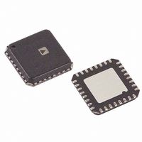
ADF4193BCPZ Analog Devices Inc, ADF4193BCPZ Datasheet - Page 24

ADF4193BCPZ
Manufacturer Part Number
ADF4193BCPZ
Description
IC PLL FREQ SYNTHESIZER 32LFCSP
Manufacturer
Analog Devices Inc
Type
Clock/Frequency Synthesizer (RF)r
Datasheet
1.ADF4193BCPZ.pdf
(28 pages)
Specifications of ADF4193BCPZ
Pll
Yes
Input
CMOS
Output
Clock
Number Of Circuits
1
Ratio - Input:output
2:1
Differential - Input:output
Yes/No
Frequency - Max
3.5GHz
Divider/multiplier
Yes/Yes
Voltage - Supply
2.7 V ~ 3.3 V
Operating Temperature
-40°C ~ 85°C
Mounting Type
Surface Mount
Package / Case
32-LFCSP
Frequency-max
3.5GHz
Pll Type
Frequency Synthesis
Frequency
3.5GHz
Supply Current
24mA
Supply Voltage Range
2.7V To 3.3V
Digital Ic Case Style
LFCSP
No. Of Pins
32
Operating Temperature Range
-40°C To +85°C
Lead Free Status / RoHS Status
Lead free / RoHS Compliant
For Use With
EVAL-ADF4193EBZ2 - BOARD EVALUATION EB2 FOR ADF4193EVAL-ADF4193EBZ1 - BOARD EVALUATION EB1 FOR ADF4193
Lead Free Status / RoHS Status
Lead free / RoHS Compliant, Lead free / RoHS Compliant
Available stocks
Company
Part Number
Manufacturer
Quantity
Price
Part Number:
ADF4193BCPZ
Manufacturer:
ADI/亚德诺
Quantity:
20 000
Company:
Part Number:
ADF4193BCPZ-RL7
Manufacturer:
AD
Quantity:
800
Part Number:
ADF4193BCPZ-RL7
Manufacturer:
ADI/亚德诺
Quantity:
20 000
ADF4193
phase swing that occurs when the BW is reduced can be
minimized.
With dither off, the fractional spur pattern due to the SDM’s
quantization noise also depends on the phase word the modulator
is seeded with. Tables of optimized FRAC and phase values for
popular SW1/SW2 and ICP timer settings can be down-loaded
from the ADF4193 product page. If making use of a phase table,
first write phase to double buffered Register R2, then write the
INT and FRAC to R0.
Avoiding Integer Boundary Channels
A further option when programming a new frequency involves
a write to Register R1 to avoid integer boundary spurs. If it is
found that the integer boundary spur level is too high, an
option is to move the integer boundary away from the desired
channel by reprogramming the R divider to select a different
PFD frequency. For example, if REF
a 26 MHz PFD reference and MOD = 130 for 200 kHz steps, the
frequency channel at 910.2 MHz has a 200 kHz integer
boundary spur because it is 200 kHz offset from 35 × 26 MHz.
An alternative way to synthesize this channel is to set R = 5 for a
20.8 MHz PFD reference and MOD = 104 for 200 kHz steps.
The 910.2 MHz channel is now 5 MHz offset from the nearest
integer multiple of 20.8 MHz and the 5 MHz beat note spurs are
IN
= 104 MHz and R = 4 for
Rev. C | Page 24 of 28
well attenuated by the loop. Setting double buffered Bit R1 [23] = 1
(CP ADJ bit) increases the charge pump current by 25%, which
compensates for the 25% increase in N with the change to the
20.8 MHz PFD frequency. This maintains constant loop dynamics
and settling time performance for jumps between the two PFD
frequencies. The CP ADJ bit should be cleared again when jumping
back to 26 MHz-based channels.
The Register R1 settings necessary for integer boundary spur
avoidance are all double buffered and do not become active on
the chip until the next write to Register R0. Register R0 should
always be the last register written to when programming a new
frequency.
Serial Interface Activity
The serial interface activity when programming the R2 or R1
registers causes no noticeable disturbance to the synthesizers
settled phase or degradation in its frequency spectrum. Therefore,
in a GSM application, it can be performed during the active
part of the data burst. Because it takes just 10.2 μs to program
the three registers, R2, R1, and R0, with the 6.5 MHz serial
interface clock rate typically used, this programming can also be
performed during the previous guard period with the LE edge
to latch in the R0 data delayed until it’s time to switch
frequency.


