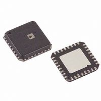
ADF4193BCPZ Analog Devices Inc, ADF4193BCPZ Datasheet - Page 20

ADF4193BCPZ
Manufacturer Part Number
ADF4193BCPZ
Description
IC PLL FREQ SYNTHESIZER 32LFCSP
Manufacturer
Analog Devices Inc
Type
Clock/Frequency Synthesizer (RF)r
Datasheet
1.ADF4193BCPZ.pdf
(28 pages)
Specifications of ADF4193BCPZ
Pll
Yes
Input
CMOS
Output
Clock
Number Of Circuits
1
Ratio - Input:output
2:1
Differential - Input:output
Yes/No
Frequency - Max
3.5GHz
Divider/multiplier
Yes/Yes
Voltage - Supply
2.7 V ~ 3.3 V
Operating Temperature
-40°C ~ 85°C
Mounting Type
Surface Mount
Package / Case
32-LFCSP
Frequency-max
3.5GHz
Pll Type
Frequency Synthesis
Frequency
3.5GHz
Supply Current
24mA
Supply Voltage Range
2.7V To 3.3V
Digital Ic Case Style
LFCSP
No. Of Pins
32
Operating Temperature Range
-40°C To +85°C
Lead Free Status / RoHS Status
Lead free / RoHS Compliant
For Use With
EVAL-ADF4193EBZ2 - BOARD EVALUATION EB2 FOR ADF4193EVAL-ADF4193EBZ1 - BOARD EVALUATION EB1 FOR ADF4193
Lead Free Status / RoHS Status
Lead free / RoHS Compliant, Lead free / RoHS Compliant
Available stocks
Company
Part Number
Manufacturer
Quantity
Price
Part Number:
ADF4193BCPZ
Manufacturer:
ADI/亚德诺
Quantity:
20 000
Company:
Part Number:
ADF4193BCPZ-RL7
Manufacturer:
AD
Quantity:
800
Part Number:
ADF4193BCPZ-RL7
Manufacturer:
ADI/亚德诺
Quantity:
20 000
ADF4193
POWER-DOWN REGISTER (R5)
R5, the power-down register (C3, C2, C1 set to 1, 0, 1, respectively)
can be used to software power down the PLL and differential
amplifier sections. After power is initially applied, there must be
writes to R5 to clear the power-down bits and to R2, R1, and R0
before the ADF4193 comes out of power-down.
Power-Down Differential Amplifier
When Bit DB6 and Bit DB7 are set high, the differential
amplifier is put into power-down. When Bit DB6 and Bit DB7
are set low, normal operation is resumed.
Power-Down Charge Pump
Setting Bit DB5 high activates a charge pump power-down and
the following events occur:
• All active dc current paths are removed, except for the
• The R and N divider counters are forced to their load state
• The charge pump is powered down with its outputs in three-
• The digital lock detect circuitry is reset.
• The RF
• The reference input buffer circuitry is disabled.
• The serial interface remains active and capable of loading and
differential amplifier.
conditions.
state mode.
latching data.
IN
input is debiased.
F5
0
1
DB7
DIFF AMP
F5
F4
0
1
PD
DIFF AMP
POWER-DOWN
DISABLED
ENABLED
DB6
F4
Figure 34. Power-Down Register (R5)
F3
0
1
DB5
F3
Rev. C | Page 20 of 28
CHARGE PUMP
POWER-DOWN
DISABLED
ENABLED
DB4
F2
F2
0
1
CHARGE PUMP
3-STATE
NORMAL OPERATION
3-STATE ENABLED
DB3
F1
F1
0
1
For normal operation, Bit DB5 should be set to 0, followed by a
write to R0.
CP Three-State
When this bit is set high, the charge pump outputs are put into
three-state. With the bit set low, the charge pump outputs are
enabled.
Counter Reset
When this bit is set to 1, the counters are held in reset. For normal
operation, this bit should be 0, followed by a write to R0.
COUNTER RESET
NORMAL OPERATION
COUNTER RESET
C3 (1)
DB2
CONTROL
C2 (0)
BITS
DB1
C1 (1)
DB0


