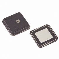
ADF4193BCPZ Analog Devices Inc, ADF4193BCPZ Datasheet - Page 6

ADF4193BCPZ
Manufacturer Part Number
ADF4193BCPZ
Description
IC PLL FREQ SYNTHESIZER 32LFCSP
Manufacturer
Analog Devices Inc
Type
Clock/Frequency Synthesizer (RF)r
Datasheet
1.ADF4193BCPZ.pdf
(28 pages)
Specifications of ADF4193BCPZ
Pll
Yes
Input
CMOS
Output
Clock
Number Of Circuits
1
Ratio - Input:output
2:1
Differential - Input:output
Yes/No
Frequency - Max
3.5GHz
Divider/multiplier
Yes/Yes
Voltage - Supply
2.7 V ~ 3.3 V
Operating Temperature
-40°C ~ 85°C
Mounting Type
Surface Mount
Package / Case
32-LFCSP
Frequency-max
3.5GHz
Pll Type
Frequency Synthesis
Frequency
3.5GHz
Supply Current
24mA
Supply Voltage Range
2.7V To 3.3V
Digital Ic Case Style
LFCSP
No. Of Pins
32
Operating Temperature Range
-40°C To +85°C
Lead Free Status / RoHS Status
Lead free / RoHS Compliant
For Use With
EVAL-ADF4193EBZ2 - BOARD EVALUATION EB2 FOR ADF4193EVAL-ADF4193EBZ1 - BOARD EVALUATION EB1 FOR ADF4193
Lead Free Status / RoHS Status
Lead free / RoHS Compliant, Lead free / RoHS Compliant
Available stocks
Company
Part Number
Manufacturer
Quantity
Price
Part Number:
ADF4193BCPZ
Manufacturer:
ADI/亚德诺
Quantity:
20 000
Company:
Part Number:
ADF4193BCPZ-RL7
Manufacturer:
AD
Quantity:
800
Part Number:
ADF4193BCPZ-RL7
Manufacturer:
ADI/亚德诺
Quantity:
20 000
ADF4193
PIN CONFIGURATION AND FUNCTION DESCRIPTIONS
Table 4. Pin Function Descriptions
Pin No.
1
2
3
4
5
6
7
8
9
10
11
12
13
14
15
16
17
18
19
20
21
22
Mnemonic
CMR
A
SW3
A
RF
RF
AV
DV
D
DV
REF
D
DV
SD
SDV
MUX
CLK
DATA
LE
V
D
A
OUT
GND
P
GND
GND
GND
GND
1
IN−
IN+
DD
GND
DD
DD
DD
IN
DD
1
2
1
1
2
3
1
2
3
OUT
Description
Common-Mode Reference Voltage for the Differential Amplifier’s Output Voltage Swing. Internally biased to
three-fifths of V
Differential Amplifier Output to Tune the External VCO.
Fast-Lock Switch 3. Closed while SW3 timeout counter is active.
Analog Ground. This is the ground return pin for the differential amplifier and the RF section.
Complementary Input to the RF Prescaler. This point must be decoupled to the ground plane with a small bypass
capacitor, typically 100 pF.
Input to the RF Prescaler. This small signal input is ac-coupled to the external VCO.
Power Supply Pin for the RF Section. Nominally 3 V. A 100 pF decoupling capacitor to the ground plane should be
placed as close as possible to this pin.
Power Supply Pin for the N Divider. Should be the same voltage as AV
should be placed as close as possible to this pin.
Ground Return Pin for DV
Power Supply Pin for the REF
should be placed as close as possible to this pin.
Reference Input. This is a CMOS input with a nominal threshold of V
100 kΩ (see Figure 15). This input can be driven from a TTL or CMOS crystal oscillator or it can be ac-coupled.
Ground Return Pin for DV
Power Supply Pin for the Serial Interface Logic. Nominally 3 V.
Ground Return Pin for the Σ-Δ Modulator.
Power Supply Pin for the Digital Σ-Δ Modulator. Nominally 3 V. A 0.1 μF decoupling capacitor to the ground plane
should be placed as close as possible to this pin.
Multiplexer Output. This multiplexer output allows either the lock detect, the scaled RF, or the scaled reference
frequency to be accessed externally (see Figure 35).
Serial Clock Input. Data is clocked into the 24-bit shift register on the CLK rising edge. This input is a high
impedance CMOS input.
Serial Data Input. The serial data is loaded MSB first with the three LSBs as the control bits. This input is a high
impedance CMOS input.
Load Enable, CMOS Input. When LE goes high, the data stored in the shift register is loaded into the register that is
selected by the three LSBs.
Power Supply Pin for the Phase Frequency Detector (PFD). Nominally 5 V, should be at the same voltage at V
A 0.1 μF decoupling capacitor to ground should be placed as close as possible to this pin.
Ground Return Pin for V
Ground Return Pin for V
P
3. Requires a 0.1 μF capacitor to ground.
NOTES:
1. THE EXPOSED PAD MUST BE CONNECTED TO AGND.
P
P
1.
2.
DV
A
AV
DD
DD
RF
RF
A
GND
CMR
SW3
OUT
DD
DD
1.
2 and DV
IN–
IN+
IN
1
1
1
Buffer and R Divider. Nominally 3 V. A 0.1 μF decoupling capacitor to ground
1
2
3
4
5
6
7
8
Figure 3. Pin Configuration
DD
Rev. C | Page 6 of 28
PIN 1
INDICATOR
3.
ADF4193
TOP VIEW
24
23
22
21
20
19
18
17
V
R
A
D
V
LE
DATA
CLK
P
P
SET
GND
GND
2
1
2
3
DD
DD
/2 and a dc equivalent input resistance of
1. A 0.1 μF decoupling capacitor to ground
P
2.


