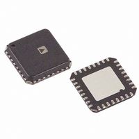
ADF4193BCPZ Analog Devices Inc, ADF4193BCPZ Datasheet - Page 5

ADF4193BCPZ
Manufacturer Part Number
ADF4193BCPZ
Description
IC PLL FREQ SYNTHESIZER 32LFCSP
Manufacturer
Analog Devices Inc
Type
Clock/Frequency Synthesizer (RF)r
Datasheet
1.ADF4193BCPZ.pdf
(28 pages)
Specifications of ADF4193BCPZ
Pll
Yes
Input
CMOS
Output
Clock
Number Of Circuits
1
Ratio - Input:output
2:1
Differential - Input:output
Yes/No
Frequency - Max
3.5GHz
Divider/multiplier
Yes/Yes
Voltage - Supply
2.7 V ~ 3.3 V
Operating Temperature
-40°C ~ 85°C
Mounting Type
Surface Mount
Package / Case
32-LFCSP
Frequency-max
3.5GHz
Pll Type
Frequency Synthesis
Frequency
3.5GHz
Supply Current
24mA
Supply Voltage Range
2.7V To 3.3V
Digital Ic Case Style
LFCSP
No. Of Pins
32
Operating Temperature Range
-40°C To +85°C
Lead Free Status / RoHS Status
Lead free / RoHS Compliant
For Use With
EVAL-ADF4193EBZ2 - BOARD EVALUATION EB2 FOR ADF4193EVAL-ADF4193EBZ1 - BOARD EVALUATION EB1 FOR ADF4193
Lead Free Status / RoHS Status
Lead free / RoHS Compliant, Lead free / RoHS Compliant
Available stocks
Company
Part Number
Manufacturer
Quantity
Price
Part Number:
ADF4193BCPZ
Manufacturer:
ADI/亚德诺
Quantity:
20 000
Company:
Part Number:
ADF4193BCPZ-RL7
Manufacturer:
AD
Quantity:
800
Part Number:
ADF4193BCPZ-RL7
Manufacturer:
ADI/亚德诺
Quantity:
20 000
ABSOLUTE MAXIMUM RATINGS
T
Table 3.
Parameter
AV
AV
V
V
Digital I/O Voltage to GND
Analog I/O Voltage to GND
REF
Operating Temperature Range
Storage Temperature Range
Maximum Junction Temperature
LFCSP θ
Reflow Soldering
P
P
A
Industrial (B Version)
Operating Temperature Range
Automotive (W Version)
(Paddle Soldered)
Peak Temperature
Time at Peak Temperature
to GND
to AV
DD
DD
= 25°C, unless otherwise noted.
IN
, RF
to GND
to DV
DD
JA
IN+
Thermal Impedance
DD
, RF
, SDV
IN−
to GND
DD
Rating
−0.3 V to +3.6 V
−0.3 V to +0.3 V
−0.3 V to +5.8 V
−0.3 V to V
−0.3 V to V
−40°C to +85°C
−40°C to +105°C
−65°C to +125°C
27.3°C/W
−0.3 V to +5.8 V
−0.3 V to V
150°C
260°C
40 sec
DD
P
DD
+ 0.3 V
+ 0.3 V
+ 0.3 V
Rev. C | Page 5 of 28
Stresses above those listed under Absolute Maximum Ratings
may cause permanent damage to the device. This is a stress
rating only; functional operation of the device at these or any
other conditions above those indicated in the operational
section of this specification is not implied. Exposure to absolute
maximum rating conditions for extended periods may affect
device reliability.
This device is a high performance RF integrated circuit with an
ESD rating of <2 kV, and it is ESD sensitive. Proper precautions
need to be taken for handling and assembly.
Transistor Count
75,800 (MOS), 545 (BJT).
ESD CAUTION
ADF4193


