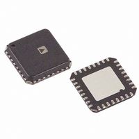
ADF4193BCPZ Analog Devices Inc, ADF4193BCPZ Datasheet - Page 21

ADF4193BCPZ
Manufacturer Part Number
ADF4193BCPZ
Description
IC PLL FREQ SYNTHESIZER 32LFCSP
Manufacturer
Analog Devices Inc
Type
Clock/Frequency Synthesizer (RF)r
Datasheet
1.ADF4193BCPZ.pdf
(28 pages)
Specifications of ADF4193BCPZ
Pll
Yes
Input
CMOS
Output
Clock
Number Of Circuits
1
Ratio - Input:output
2:1
Differential - Input:output
Yes/No
Frequency - Max
3.5GHz
Divider/multiplier
Yes/Yes
Voltage - Supply
2.7 V ~ 3.3 V
Operating Temperature
-40°C ~ 85°C
Mounting Type
Surface Mount
Package / Case
32-LFCSP
Frequency-max
3.5GHz
Pll Type
Frequency Synthesis
Frequency
3.5GHz
Supply Current
24mA
Supply Voltage Range
2.7V To 3.3V
Digital Ic Case Style
LFCSP
No. Of Pins
32
Operating Temperature Range
-40°C To +85°C
Lead Free Status / RoHS Status
Lead free / RoHS Compliant
For Use With
EVAL-ADF4193EBZ2 - BOARD EVALUATION EB2 FOR ADF4193EVAL-ADF4193EBZ1 - BOARD EVALUATION EB1 FOR ADF4193
Lead Free Status / RoHS Status
Lead free / RoHS Compliant, Lead free / RoHS Compliant
Available stocks
Company
Part Number
Manufacturer
Quantity
Price
Part Number:
ADF4193BCPZ
Manufacturer:
ADI/亚德诺
Quantity:
20 000
Company:
Part Number:
ADF4193BCPZ-RL7
Manufacturer:
AD
Quantity:
800
Part Number:
ADF4193BCPZ-RL7
Manufacturer:
ADI/亚德诺
Quantity:
20 000
MUX REGISTER (R6)
With C3, C2, and C1 set to 1, 1, 0, respectively, the MUX
register is programmed.
Σ-Δ and Lock Detect Modes
Bit DB15 to Bit DB12 are used to reconfigure certain PLL
operating modes. In the initialization sequence after power is
applied to the chip, the four bits must first be programmed to
all zeros. This initializes the PLL to a known state with dither
off in the Σ-Δ modulator and a 3 ns PFD error threshold in the
lock detect circuit.
To turn on dither in the Σ-Δ modulator, an additional write
should be made to Register R6 to program bits [DB15:DB12] =
[0011]. However, for lowest noise operation, it is best to leave
dither off.
To change the lock detect threshold from 3 ns to 10 ns, a
separate write to R6 should be performed to program bits
[DB15:DB12] = [1001]. This should be done for reliable lock
detect operation when the RF frequency is <2 GHz.
A write to R6 that programs bits [DB15:DB12] = [0000] returns
operation to the default state with both dither off and a 3 ns
lock detect threshold.
Reserved Bits
The reserved bits must all be set to 0 for normal operation.
DB15
M13
0
0
1
M13
LOCK DETECT MODES
ALL OTHER STATES
SIGMA-DELTA
DB14
M12
M12
0
0
0
AND
DB13
M11
M11
0
1
0
DB12
M10
M10
0
1
1
DB11
0
SIGMA-DELTA MODES
INIT STATE, DITHER OFF,
3ns LOCK DETECT THRESHOLD
DITHER ON
10ns LOCK DETECT THRESHOLD
RESERVED
DB10
0
RESERVED
Figure 35. MUX Register (R6)
DB9
0
Rev. C | Page 21 of 28
DB8
0
DB7
0
MUX
These bits control the on-chip multiplexer. See Figure 35 for the
truth table. This pin is useful for diagnosis because it allows the
user to look at various internal points of the chip, such as the
R divider and INT divider outputs.
In addition, it is possible to monitor the programmed timeout
counter intervals on MUX
counter was programmed to 65 (with a 26 MHz PFD), then
following the next write to R0, a pulse width of 10 μs would be
observed on the MUX
Digital lock detect is available via the MUX
DB6
M4
M4
0
0
0
0
0
0
0
0
1
1
1
1
1
1
1
1
OUT
DB5
M3
MUX
M3
0
0
0
0
1
1
1
1
0
0
0
0
1
1
1
1
Modes
OUT
DB4
M2
0
0
1
1
0
0
1
1
0
0
1
1
0
0
1
1
M2
M1
0
1
0
1
0
1
0
1
0
1
0
1
0
1
0
1
DB3
M1
MUX
3-STATE
DIGITAL LOCK DETECT
N DIVIDER OUTPUT
LOGIC HIGH
R COUNTER
RESERVED
SERIAL DATA OUT
LOGIC LOW
R DIVIDER/2 OUTPUT
N DIVIDER/2 OUTPUT
RESERVED
RESERVED
ICP TIMEOUT SIGNAL
SW1/2 TIMEOUT SIGNAL
SW3 TIMEOUT SIGNAL
RESERVED
OUT
C3 (1)
DB2
OUT
pin.
OUT
CONTROL
C2 (1)
. For example, if the ICP timeout
BITS
DB1
C1 (0)
DB0
OUT
pin.
ADF4193


