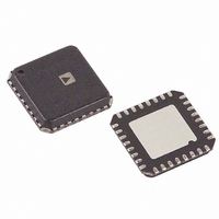
ADF4193BCPZ Analog Devices Inc, ADF4193BCPZ Datasheet - Page 22

ADF4193BCPZ
Manufacturer Part Number
ADF4193BCPZ
Description
IC PLL FREQ SYNTHESIZER 32LFCSP
Manufacturer
Analog Devices Inc
Type
Clock/Frequency Synthesizer (RF)r
Datasheet
1.ADF4193BCPZ.pdf
(28 pages)
Specifications of ADF4193BCPZ
Pll
Yes
Input
CMOS
Output
Clock
Number Of Circuits
1
Ratio - Input:output
2:1
Differential - Input:output
Yes/No
Frequency - Max
3.5GHz
Divider/multiplier
Yes/Yes
Voltage - Supply
2.7 V ~ 3.3 V
Operating Temperature
-40°C ~ 85°C
Mounting Type
Surface Mount
Package / Case
32-LFCSP
Frequency-max
3.5GHz
Pll Type
Frequency Synthesis
Frequency
3.5GHz
Supply Current
24mA
Supply Voltage Range
2.7V To 3.3V
Digital Ic Case Style
LFCSP
No. Of Pins
32
Operating Temperature Range
-40°C To +85°C
Lead Free Status / RoHS Status
Lead free / RoHS Compliant
For Use With
EVAL-ADF4193EBZ2 - BOARD EVALUATION EB2 FOR ADF4193EVAL-ADF4193EBZ1 - BOARD EVALUATION EB1 FOR ADF4193
Lead Free Status / RoHS Status
Lead free / RoHS Compliant, Lead free / RoHS Compliant
Available stocks
Company
Part Number
Manufacturer
Quantity
Price
Part Number:
ADF4193BCPZ
Manufacturer:
ADI/亚德诺
Quantity:
20 000
Company:
Part Number:
ADF4193BCPZ-RL7
Manufacturer:
AD
Quantity:
800
Part Number:
ADF4193BCPZ-RL7
Manufacturer:
ADI/亚德诺
Quantity:
20 000
ADF4193
PROGRAMMING
The ADF4193 can synthesize output frequencies with a channel
step or resolution that is a fraction of the input reference frequency.
For a given input reference frequency and a desired output
frequency step, the first choice to make is the PFD reference
frequency and the MOD. Once these are chosen, the desired
output frequency channels are set by programming the INT
and FRAC values.
WORKED EXAMPLE
In this example of a GSM900 RX system, it is required to
generate RF output frequencies with channel steps of 200 kHz.
A 104 MHz reference frequency input (REF
R divider setting that set the PFD reference is shown in
Equation 1.
where:
REF
D is the doubler enable bit (0 or 1).
R is the 4-bit R counter code (0…15).
T is the REF/2 bit (0 or 1).
The maximum PFD reference frequency of 26 MHz is chosen
and the following settings are programmed to give an R divider
value of 4:
Doubler enable = 0
R = 2
REF/2 = 1
Next, the modulus is chosen to allow fractional steps of 200 kHz.
Once the channel step is defined, the following equation shows
how output frequency channels are programmed:
where:
RF
INT is the integer part of the division.
FRAC is the numerator part of the fractional division.
MOD is the modulus or denominator part of the fractional
division.
For example, the frequency channel at 962.4 MHz is synthesized
by programming the following values:
INT = 37
FRAC = 2
OUT
IN
F
MOD = 26 MHz/200 kHz = 130
RF
PFD
is the input reference frequency.
is the desired RF output frequency.
OUT
= REF
= [INT + (FRAC/MOD] × [F
IN
× [(1 + D)/(R × (1 + T))]
PFD
]
IN
) is available. The
Rev. C | Page 22 of 28
(1)
(2)
(3)
SPUR MECHANISMS
The Fractional Spurs, Integer Boundary Spurs, and Reference
Spurs sections describe the three different spur mechanisms
that arise with a fractional-N synthesizer and how the ADF4193
can be programmed to minimize them.
Fractional Spurs
The fractional interpolator in the ADF4193 is a third-order, Σ-Δ
modulator (SDM) with a modulus (MOD) that is programmable to
any integer value from 13 to 4095. If dither is enabled, then the
minimum allowed value of MOD is 50. The SDM is clocked at
the PFD reference rate (f
to be synthesized at a channel step resolution of f
With dither turned off, the quantization noise from the Σ-Δ
modulator appears as fractional spurs. The interval between
spurs is f
in the digital Σ-Δ modulator. For the third-order modulator
used in the ADF4193, the repeat length depends on the value of
MOD, as shown in Table 7.
Table 7. Fractional Spurs with Dither Off
Condition (Dither Off)
If MOD is divisible by 2,
If MOD is divisible by 3,
If MOD is divisible by 6
Otherwise
With dither enabled, the repeat length is extended to 221 cycles,
regardless of the value of MOD, which makes the quantization
error spectrum look like broadband noise. This can degrade
the in-band phase noise at the PLL output by as much as 10 dB.
Therefore, for the lowest noise, dither off is a better choice,
particularly when the final loop BW is low enough to attenuate
even the lowest frequency fractional spur. The wide loop
bandwidth range available with the ADF4193 makes this
possible in most applications.
Integer Boundary Spurs
Another mechanism for fractional spur creation involves
interactions between the RF VCO frequency and the reference
frequency. When these frequencies are not integer related, spur
sidebands appear on the VCO output spectrum at an offset
frequency that corresponds to the beat note or difference
frequency between an integer multiple of the reference and the
VCO frequency.
These spurs are attenuated by the loop filter and are more
noticeable on channels close to integer multiples of the refer-
ence where the difference frequency can be inside the loop
bandwidth, thus the name integer boundary spurs.
but not 3
but not 2
PFD
/L, where L is the repeat length of the code sequence
PFD
) that allows PLL output frequencies
Repeat Length
2 × MOD
3 × MOD
6 × MOD
MOD
Spur Interval
Channel step/2
Channel step/3
Channel step/6
Channel step
PFD
/MOD.


