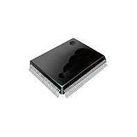
SAA7115HLBE NXP Semiconductors, SAA7115HLBE Datasheet - Page 286

SAA7115HLBE
Manufacturer Part Number
SAA7115HLBE
Description
Video ICs ADV DGTL VIDEO DECODR
Manufacturer
NXP Semiconductors
Datasheet
1.SAA7115HLBE.pdf
(548 pages)
Specifications of SAA7115HLBE
Operating Supply Voltage
3.3 V
Maximum Operating Temperature
+ 70 C
Package / Case
SOT-407
Minimum Operating Temperature
0 C
Mounting Style
SMD/SMT
Number Of Channels
2
Resolution
8 bit
Lead Free Status / RoHS Status
Lead free / RoHS Compliant
Other names
SAA7115HL/V1,557 SAF7115HLBE
- Current page: 286 of 548
- Download datasheet (6Mb)
PNX1300/01/02/11 Data Book
PCI transfer and is incremented for each PCI word trans-
ferred.
The XIO Bus does not generate parity during XIO Bus
write transfers or check parity during XIO Bus read trans-
fers. This allows the XIO Bus to interface to standard 8-
bit devices without having to add parity-generation and
check logic. While the XIO Bus is active, the XIO Bus log-
ic inhibits parity checking and drives the PCI Parity and
Parity Error pins so that they do not float.
Word transfer is used to transfer the bytes to and from
the PCI bus for hardware simplicity. The primary intend-
ed use of the PCI-XIO Bus is for slow devices, ROMs,
flash EPROMs and I/O. Because the PCI-XIO bus is so
22-2
Figure 22-1. Partial PNX1300 chip block diagram
Digital
Camera
DMSD
or Raw
Video
Digital
Audio
Serial
JTAG
Clock
XIO Bus
Controls
PRELIMINARY SPECIFICATION
Video In
Audio In
Audio Out
2.5 GOPS
Glueless
Flash
EPROM I/F
DSPCPU
400 MIPS
PCI - XIO Bus AD[31:0]
PCI and External I/O (PCI-XIO) Bus Interface
D$
I$
SDRAM
Highway
SDRAM: 32-bit data
XIO
I/O Device
MMI
much slower than the PNX1300, there is time available
for the PNX1300 to pack and unpack the words. In the
case of ROMs and flash EPROMs, the data is typically
compressed, requiring the PNX1300 CPU to both un-
pack and decompress the data.
The PCI-XIO Bus Controller logic reconfigures the byte
enables as control signals for the attached XIO Bus chips
during XIO Bus transfers. It also drives the PCI_TRDY#
signal to the PCI Bus for each transfer. The PCI Bus byte
enables are reconfigured to generate XIO Bus timing sig-
nals: Read (IORD), Write (IOWR) and Data Strobe (DS).
These signals allow ROM, flash EPROM, 68K and x86
devices to be gluelessly interfaced to the XIO Bus. For a
single device, the PCI_INTB# line is used as the global
Synchronous
Serial I/F
I
Co Processor
2
Video Out
VLD Assist
C Interface
PNX1300
PCI
I/O Device
Image
Philips Semiconductors
PCI Bus
Controls
V.34 Modem
Video Out
I
CCIR 601
Digital
2
C Bus
Related parts for SAA7115HLBE
Image
Part Number
Description
Manufacturer
Datasheet
Request
R
Part Number:
Description:
Ntsc/pal/secam 9-bit Video Decoder
Manufacturer:
NXP Semiconductors
Datasheet:
Part Number:
Description:
NXP Semiconductors designed the LPC2420/2460 microcontroller around a 16-bit/32-bitARM7TDMI-S CPU core with real-time debug interfaces that include both JTAG andembedded trace
Manufacturer:
NXP Semiconductors
Datasheet:

Part Number:
Description:
NXP Semiconductors designed the LPC2458 microcontroller around a 16-bit/32-bitARM7TDMI-S CPU core with real-time debug interfaces that include both JTAG andembedded trace
Manufacturer:
NXP Semiconductors
Datasheet:
Part Number:
Description:
NXP Semiconductors designed the LPC2468 microcontroller around a 16-bit/32-bitARM7TDMI-S CPU core with real-time debug interfaces that include both JTAG andembedded trace
Manufacturer:
NXP Semiconductors
Datasheet:
Part Number:
Description:
NXP Semiconductors designed the LPC2470 microcontroller, powered by theARM7TDMI-S core, to be a highly integrated microcontroller for a wide range ofapplications that require advanced communications and high quality graphic displays
Manufacturer:
NXP Semiconductors
Datasheet:
Part Number:
Description:
NXP Semiconductors designed the LPC2478 microcontroller, powered by theARM7TDMI-S core, to be a highly integrated microcontroller for a wide range ofapplications that require advanced communications and high quality graphic displays
Manufacturer:
NXP Semiconductors
Datasheet:
Part Number:
Description:
The Philips Semiconductors XA (eXtended Architecture) family of 16-bit single-chip microcontrollers is powerful enough to easily handle the requirements of high performance embedded applications, yet inexpensive enough to compete in the market for hi
Manufacturer:
NXP Semiconductors
Datasheet:
Part Number:
Description:
The XA-S3 device is a member of Philips Semiconductors? XA(eXtended Architecture) family of high performance 16-bitsingle-chip microcontrollers
Manufacturer:
NXP Semiconductors
Datasheet:

Part Number:
Description:
The NXP BlueStreak LH75401/LH75411 family consists of two low-cost 16/32-bit System-on-Chip (SoC) devices
Manufacturer:
NXP Semiconductors
Datasheet:

Part Number:
Description:
The NXP LPC3130/3131 combine an 180 MHz ARM926EJ-S CPU core, high-speed USB2
Manufacturer:
NXP Semiconductors
Datasheet:

Part Number:
Description:
The NXP LPC3141 combine a 270 MHz ARM926EJ-S CPU core, High-speed USB 2
Manufacturer:
NXP Semiconductors

Part Number:
Description:
The NXP LPC3143 combine a 270 MHz ARM926EJ-S CPU core, High-speed USB 2
Manufacturer:
NXP Semiconductors

Part Number:
Description:
The NXP LPC3152 combines an 180 MHz ARM926EJ-S CPU core, High-speed USB 2
Manufacturer:
NXP Semiconductors

Part Number:
Description:
The NXP LPC3154 combines an 180 MHz ARM926EJ-S CPU core, High-speed USB 2
Manufacturer:
NXP Semiconductors


