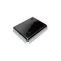
SAA7115HLBE NXP Semiconductors, SAA7115HLBE Datasheet - Page 100

SAA7115HLBE
Manufacturer Part Number
SAA7115HLBE
Description
Video ICs ADV DGTL VIDEO DECODR
Manufacturer
NXP Semiconductors
Datasheet
1.SAA7115HLBE.pdf
(548 pages)
Specifications of SAA7115HLBE
Operating Supply Voltage
3.3 V
Maximum Operating Temperature
+ 70 C
Package / Case
SOT-407
Minimum Operating Temperature
0 C
Mounting Style
SMD/SMT
Number Of Channels
2
Resolution
8 bit
Lead Free Status / RoHS Status
Lead free / RoHS Compliant
Other names
SAA7115HL/V1,557 SAF7115HLBE
- Current page: 100 of 548
- Download datasheet (6Mb)
PNX1300/01/02/11 Data Book
Figure 6-4. VI connected to a 10-bit video A/D converter.
6.2
The VI block can operate in two distinct clocking modes,
as controlled by the VI_CLOCK control register (see
Figure
SELFCLOCK = 0: ‘External clocking mode’. This is the
most common mode of operation. In this mode, the
VI_CLK pin is an asynchronous clock input. All other in-
puts are sampled on positive edges of the VI_CLK clock
signal. On-chip synchronizers ensure reliable asynchro-
nous capture. This mode can be combined with DIAG-
MODE, in which case the EVO clock acts as the asyn-
chronous clock source. In external clocking mode, the
value of DIVIDER is ignored.
SELFCLOCK = 1: ‘Internal clocking mode”. This
mode is typically intended for use with external A/D con-
verters or other sources that require a clock. In this
mode, VI_CLK is an output pin. Positive edges of
VI_CLK are used to sample all other inputs. The gener-
ated clock frequency can be programmed using the DI-
VIDER field in the VI_CLOCK register.
On RESET, VI_CLOCK is set to zero, i.e. external clock-
ing mode is the default with DIVIDER ignored.
Figure 6-5. Camera YUV 4:2:2 sampling (co-sited luminance/chrominance).
6-4
6-11).
CLOCK GENERATOR
f
VICLK
Analog video
PRELIMINARY SPECIFICATION
=
----------------------- -
DIVIDER
f
DSPCPU
Chrominance (U,V)
samples
10-bit Video A/D
6.3
In fullres capture mode, the VI unit receives all three vid-
eo components Y, U, and V, as well as synchronization
information (SAV and EAV codes) on the VI_DATA[7:0]
pins in CCIR656 format. See
components Y, U, and V are separated into three differ-
ent streams. Each component is written in packed form
into separate Y, U, and V buffers in the SDRAM. This is
commonly called a planar format
The CCIR656 standard specifies that the camera has to
obey the sampling rules illustrated in
pable of chrominance resampling, and can produce sam-
ples in memory in two ways:
VI_CTL.SC=0. ‘Co-sited sampling’ places luminance
and chrominance samples in memory without any modi-
fication. Hence, a planar format results with sampling po-
sitions as per co-sited luminance and chrominance YUV
4:2:2 convention.
Luminance
1.
samples
logic ‘1’
The planar format is most suitable as input to software
compression algorithms.
FULLRES CAPTURE MODE
VI_DATA[9:0]
VI_DVALID
VI_CLK
PNX1300
Philips Semiconductors
Figure
1
(see
6-8. The three video
Figure
Figure
6-5. VI is ca-
6-10).
Related parts for SAA7115HLBE
Image
Part Number
Description
Manufacturer
Datasheet
Request
R
Part Number:
Description:
Ntsc/pal/secam 9-bit Video Decoder
Manufacturer:
NXP Semiconductors
Datasheet:
Part Number:
Description:
NXP Semiconductors designed the LPC2420/2460 microcontroller around a 16-bit/32-bitARM7TDMI-S CPU core with real-time debug interfaces that include both JTAG andembedded trace
Manufacturer:
NXP Semiconductors
Datasheet:

Part Number:
Description:
NXP Semiconductors designed the LPC2458 microcontroller around a 16-bit/32-bitARM7TDMI-S CPU core with real-time debug interfaces that include both JTAG andembedded trace
Manufacturer:
NXP Semiconductors
Datasheet:
Part Number:
Description:
NXP Semiconductors designed the LPC2468 microcontroller around a 16-bit/32-bitARM7TDMI-S CPU core with real-time debug interfaces that include both JTAG andembedded trace
Manufacturer:
NXP Semiconductors
Datasheet:
Part Number:
Description:
NXP Semiconductors designed the LPC2470 microcontroller, powered by theARM7TDMI-S core, to be a highly integrated microcontroller for a wide range ofapplications that require advanced communications and high quality graphic displays
Manufacturer:
NXP Semiconductors
Datasheet:
Part Number:
Description:
NXP Semiconductors designed the LPC2478 microcontroller, powered by theARM7TDMI-S core, to be a highly integrated microcontroller for a wide range ofapplications that require advanced communications and high quality graphic displays
Manufacturer:
NXP Semiconductors
Datasheet:
Part Number:
Description:
The Philips Semiconductors XA (eXtended Architecture) family of 16-bit single-chip microcontrollers is powerful enough to easily handle the requirements of high performance embedded applications, yet inexpensive enough to compete in the market for hi
Manufacturer:
NXP Semiconductors
Datasheet:
Part Number:
Description:
The XA-S3 device is a member of Philips Semiconductors? XA(eXtended Architecture) family of high performance 16-bitsingle-chip microcontrollers
Manufacturer:
NXP Semiconductors
Datasheet:

Part Number:
Description:
The NXP BlueStreak LH75401/LH75411 family consists of two low-cost 16/32-bit System-on-Chip (SoC) devices
Manufacturer:
NXP Semiconductors
Datasheet:

Part Number:
Description:
The NXP LPC3130/3131 combine an 180 MHz ARM926EJ-S CPU core, high-speed USB2
Manufacturer:
NXP Semiconductors
Datasheet:

Part Number:
Description:
The NXP LPC3141 combine a 270 MHz ARM926EJ-S CPU core, High-speed USB 2
Manufacturer:
NXP Semiconductors

Part Number:
Description:
The NXP LPC3143 combine a 270 MHz ARM926EJ-S CPU core, High-speed USB 2
Manufacturer:
NXP Semiconductors

Part Number:
Description:
The NXP LPC3152 combines an 180 MHz ARM926EJ-S CPU core, High-speed USB 2
Manufacturer:
NXP Semiconductors

Part Number:
Description:
The NXP LPC3154 combines an 180 MHz ARM926EJ-S CPU core, High-speed USB 2
Manufacturer:
NXP Semiconductors


