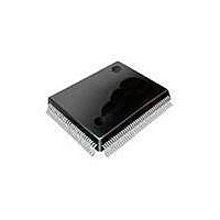
SAA7115HLBE NXP Semiconductors, SAA7115HLBE Datasheet - Page 135

SAA7115HLBE
Manufacturer Part Number
SAA7115HLBE
Description
Video ICs ADV DGTL VIDEO DECODR
Manufacturer
NXP Semiconductors
Datasheet
1.SAA7115HLBE.pdf
(548 pages)
Specifications of SAA7115HLBE
Operating Supply Voltage
3.3 V
Maximum Operating Temperature
+ 70 C
Package / Case
SOT-407
Minimum Operating Temperature
0 C
Mounting Style
SMD/SMT
Number Of Channels
2
Resolution
8 bit
Lead Free Status / RoHS Status
Lead free / RoHS Compliant
Other names
SAA7115HL/V1,557 SAF7115HLBE
- Current page: 135 of 548
- Download datasheet (6Mb)
Philips Semiconductors
The EVO block can be separately powered down by set-
ting a bit in the BLOCK_POWER_DOWN register. Refer
to
It is recommended that EVO be stopped (by negating
VO_CTL. ENABLE) before block level power down is
started, or that SLEEPLESS mode is used when global
power down is activated.
7.19
The PLL filter reduces the phase jitter of the DDS synthe-
sizer output. It can also be used to multiply the DDS out-
put frequency by 2×. The DDS and PLL filter together
provide a high-quality, accurately-programmable output
video clock. The PLL filter block is shown in
At hardware reset, the output multiplexer is set to 0x3,
and the PLL system is disabled. To start the PLL system,
the following steps must be performed:
1. Assign a DDS frequency. This starts the DDS. Allow
2. Choose a value for PLL_S and PLL_T. For 8-40 MHz
Table 7-12. DDS and PLL example settings
Figure 7-32. PLL filter block diagram.
4 – 10 MHz
8 – 45 MHz
40 – 81 MHz
9 × CPU Clock
Chapter 21, “Power Management.”
Frequency
for at least 31 DSPCPU cycles for the DDS frequency
setting to take effect.
operation, a value of 1 (which selects division by 2) is
recommended.
Desired
31
Square-Wave DDS
DDS AND PLL FILTER DETAILS
FREQUENCY
8 – 20 MHz
8 – 45 MHz
20 – 40. 5 MHz
DDS frequency
0
div S+1
1 (divide by 2)
1 (divide by 2)
1 (divide by 2)
PLL_S
PLL_S
Figure
Detect
Phase
1 (divide by 2)
1 (divide by 2)
3 (divide by 4)
7-32.
PLL_T
div T+1
3. Choose a value for CLOCK_SELECT. For 8-81 MHz
4. Assign values to the VO_CTL register containing the
Once the PLL is locked, small changes to the DDS fre-
quency are allowed, and the VO_CLK output will
smoothly track the frequency change.
Note: Most consumer electronics equipment imposes
very high precision requirements on the value of the col-
or burst frequency. A video encoder will derive the color
burst frequency from VO_CLK. When changing the
VO_CLK frequency in software to phase-lock the EVO to
a master reference, special care is required to keep the
color burst signal frequency within a tolerance of about
50 ppm. When using a Philips DENC (Digital Encoder),
the color burst frequency is derived from the master
DENC frequency by a programmable synthesizer on the
DENC chip. In this case, VO_CLK changes larger than
50 ppm are allowed by changing the DENC synthesizer
over its I
change.
Table 7-12
PRELIMINARY SPECIFICATION
Loop
Filter
PLL_T
operation, CLOCK_SELECT = 00 is recommended.
above choices. The first assignment with
CLOCK_SELECT not equal to 0x3 enables the PLL
system. Allow for a maximum of 50 microseconds to
achieve lock.
01 (T divider)
00 (VCO)
00 (VCO)
CLOCK_SELECT
2
C interface to compensate for the VO_CLK
illustrates recommended settings.
8–90 MHz
VCO
Standard or 16:9 digital video
Custom low speed video
High pixel rate custom video
CLOCK_SELECT
00
01
10
11
CLKOUT
Enhanced Video Out
Usage
(to Frame Timing Gen.)
VO_CLK Internal
VO_CLK
7-25
Related parts for SAA7115HLBE
Image
Part Number
Description
Manufacturer
Datasheet
Request
R
Part Number:
Description:
Ntsc/pal/secam 9-bit Video Decoder
Manufacturer:
NXP Semiconductors
Datasheet:
Part Number:
Description:
NXP Semiconductors designed the LPC2420/2460 microcontroller around a 16-bit/32-bitARM7TDMI-S CPU core with real-time debug interfaces that include both JTAG andembedded trace
Manufacturer:
NXP Semiconductors
Datasheet:

Part Number:
Description:
NXP Semiconductors designed the LPC2458 microcontroller around a 16-bit/32-bitARM7TDMI-S CPU core with real-time debug interfaces that include both JTAG andembedded trace
Manufacturer:
NXP Semiconductors
Datasheet:
Part Number:
Description:
NXP Semiconductors designed the LPC2468 microcontroller around a 16-bit/32-bitARM7TDMI-S CPU core with real-time debug interfaces that include both JTAG andembedded trace
Manufacturer:
NXP Semiconductors
Datasheet:
Part Number:
Description:
NXP Semiconductors designed the LPC2470 microcontroller, powered by theARM7TDMI-S core, to be a highly integrated microcontroller for a wide range ofapplications that require advanced communications and high quality graphic displays
Manufacturer:
NXP Semiconductors
Datasheet:
Part Number:
Description:
NXP Semiconductors designed the LPC2478 microcontroller, powered by theARM7TDMI-S core, to be a highly integrated microcontroller for a wide range ofapplications that require advanced communications and high quality graphic displays
Manufacturer:
NXP Semiconductors
Datasheet:
Part Number:
Description:
The Philips Semiconductors XA (eXtended Architecture) family of 16-bit single-chip microcontrollers is powerful enough to easily handle the requirements of high performance embedded applications, yet inexpensive enough to compete in the market for hi
Manufacturer:
NXP Semiconductors
Datasheet:
Part Number:
Description:
The XA-S3 device is a member of Philips Semiconductors? XA(eXtended Architecture) family of high performance 16-bitsingle-chip microcontrollers
Manufacturer:
NXP Semiconductors
Datasheet:

Part Number:
Description:
The NXP BlueStreak LH75401/LH75411 family consists of two low-cost 16/32-bit System-on-Chip (SoC) devices
Manufacturer:
NXP Semiconductors
Datasheet:

Part Number:
Description:
The NXP LPC3130/3131 combine an 180 MHz ARM926EJ-S CPU core, high-speed USB2
Manufacturer:
NXP Semiconductors
Datasheet:

Part Number:
Description:
The NXP LPC3141 combine a 270 MHz ARM926EJ-S CPU core, High-speed USB 2
Manufacturer:
NXP Semiconductors

Part Number:
Description:
The NXP LPC3143 combine a 270 MHz ARM926EJ-S CPU core, High-speed USB 2
Manufacturer:
NXP Semiconductors

Part Number:
Description:
The NXP LPC3152 combines an 180 MHz ARM926EJ-S CPU core, High-speed USB 2
Manufacturer:
NXP Semiconductors

Part Number:
Description:
The NXP LPC3154 combines an 180 MHz ARM926EJ-S CPU core, High-speed USB 2
Manufacturer:
NXP Semiconductors


