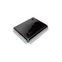
SAA7115HLBE NXP Semiconductors, SAA7115HLBE Datasheet - Page 186

SAA7115HLBE
Manufacturer Part Number
SAA7115HLBE
Description
Video ICs ADV DGTL VIDEO DECODR
Manufacturer
NXP Semiconductors
Datasheet
1.SAA7115HLBE.pdf
(548 pages)
Specifications of SAA7115HLBE
Operating Supply Voltage
3.3 V
Maximum Operating Temperature
+ 70 C
Package / Case
SOT-407
Minimum Operating Temperature
0 C
Mounting Style
SMD/SMT
Number Of Channels
2
Resolution
8 bit
Lead Free Status / RoHS Status
Lead free / RoHS Compliant
Other names
SAA7115HL/V1,557 SAF7115HLBE
- Current page: 186 of 548
- Download datasheet (6Mb)
PNX1300/01/02/11 Data Book
Table 12-6. Memory Configuration Registers
Table 12-7. MM_CONFIG Fields
12.6.2
The PLL_RATIOS register controls the operation of the
separate memory-interface and CPU PLLs. Fields in this
register determine if the PLLs are active and what in-
12-4
Figure 12-2. Memory interface configuration registers.
Figure 12-3. PNX1300 memory and core PLL connections.
MM_CONFIG
PLL_RATIOS
REFRESH Refresh interval in memory clock cycles.
MMIO_base
Field
0x10 0100
0x10 0300
SIZE
Register
offset:
Memory System Clocks
External Clock Input
PLL_RATIOS Register
Default value 1000 (0x03E8).
Memory rank size
TRI_CLKIN
MM_CLK1
MM_CLK0
MM_CONFIG (r/o)
PLL_RATIOS (r/o)
Describes external memory configuration
Controls separate memory and CPU PLLs
(phase-locked loops)
PRELIMINARY SPECIFICATION
Function
Purpose
Memory System
31
31
SD SB CD CB SR
7
0
1
2
3
4
5
6
7
6
PLL
Reserved
512KB
1MB
2MB
4MB
8MB
16MB
32MB
5
4
3
2
CR
0
PLL_RATIOS Register
Table 12-8. PLL_RATIOS Fields
put:output ratio each PLL should generate.
summarizes the field functions.
the PLLs are connected and how fields in the
PLL_RATIOS register control them. For normal opera-
Field
CR
CD
SR
CB
SD
SB
19
CPU:memory ratio
Memory:external ratio
CPU PLL Disable
CPU PLL bypass
SDRAM PLL Disable
SDRAM PLL bypass
DSPCPU PLL
TO DDSes && EVO PLL
SDRAM PLL Bypass
SDRAM PLL Disable
x3, x9
REFRESH
CPU PLL Bypass
16-bit memory interface
CPU PLL Disable
Philips Semiconductors
Function
SDRAM Ratio
5–7 Reserved
0
1
2
3
4
0
1
0
1
0
1
0
1
0
1
Figure 12-3
SB SD CB CD SR
7
1:1
2:1
3:2
4:3
5:4
2:1
3:1
CPU PLL on
CPU PLL off
CPU ← PLL
CPU ← Memory
SDRAM PLL on
SDRAM PLL off
Memory ← PLL
Memory ← external
PNX1300
CPU Ratio
6
PNX1300
Peripheral
Clocks
5
PNX1300
Core
Clock
4
4
BW
3
3
shows how
Table 12-8
2
2
SIZE
CR
0
0
Related parts for SAA7115HLBE
Image
Part Number
Description
Manufacturer
Datasheet
Request
R
Part Number:
Description:
Ntsc/pal/secam 9-bit Video Decoder
Manufacturer:
NXP Semiconductors
Datasheet:
Part Number:
Description:
NXP Semiconductors designed the LPC2420/2460 microcontroller around a 16-bit/32-bitARM7TDMI-S CPU core with real-time debug interfaces that include both JTAG andembedded trace
Manufacturer:
NXP Semiconductors
Datasheet:

Part Number:
Description:
NXP Semiconductors designed the LPC2458 microcontroller around a 16-bit/32-bitARM7TDMI-S CPU core with real-time debug interfaces that include both JTAG andembedded trace
Manufacturer:
NXP Semiconductors
Datasheet:
Part Number:
Description:
NXP Semiconductors designed the LPC2468 microcontroller around a 16-bit/32-bitARM7TDMI-S CPU core with real-time debug interfaces that include both JTAG andembedded trace
Manufacturer:
NXP Semiconductors
Datasheet:
Part Number:
Description:
NXP Semiconductors designed the LPC2470 microcontroller, powered by theARM7TDMI-S core, to be a highly integrated microcontroller for a wide range ofapplications that require advanced communications and high quality graphic displays
Manufacturer:
NXP Semiconductors
Datasheet:
Part Number:
Description:
NXP Semiconductors designed the LPC2478 microcontroller, powered by theARM7TDMI-S core, to be a highly integrated microcontroller for a wide range ofapplications that require advanced communications and high quality graphic displays
Manufacturer:
NXP Semiconductors
Datasheet:
Part Number:
Description:
The Philips Semiconductors XA (eXtended Architecture) family of 16-bit single-chip microcontrollers is powerful enough to easily handle the requirements of high performance embedded applications, yet inexpensive enough to compete in the market for hi
Manufacturer:
NXP Semiconductors
Datasheet:
Part Number:
Description:
The XA-S3 device is a member of Philips Semiconductors? XA(eXtended Architecture) family of high performance 16-bitsingle-chip microcontrollers
Manufacturer:
NXP Semiconductors
Datasheet:

Part Number:
Description:
The NXP BlueStreak LH75401/LH75411 family consists of two low-cost 16/32-bit System-on-Chip (SoC) devices
Manufacturer:
NXP Semiconductors
Datasheet:

Part Number:
Description:
The NXP LPC3130/3131 combine an 180 MHz ARM926EJ-S CPU core, high-speed USB2
Manufacturer:
NXP Semiconductors
Datasheet:

Part Number:
Description:
The NXP LPC3141 combine a 270 MHz ARM926EJ-S CPU core, High-speed USB 2
Manufacturer:
NXP Semiconductors

Part Number:
Description:
The NXP LPC3143 combine a 270 MHz ARM926EJ-S CPU core, High-speed USB 2
Manufacturer:
NXP Semiconductors

Part Number:
Description:
The NXP LPC3152 combines an 180 MHz ARM926EJ-S CPU core, High-speed USB 2
Manufacturer:
NXP Semiconductors

Part Number:
Description:
The NXP LPC3154 combines an 180 MHz ARM926EJ-S CPU core, High-speed USB 2
Manufacturer:
NXP Semiconductors


