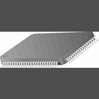
CR16MCS9VJE8 National Semiconductor, CR16MCS9VJE8 Datasheet - Page 95

CR16MCS9VJE8
Manufacturer Part Number
CR16MCS9VJE8
Description
16-Bit Microcontroller IC
Manufacturer
National Semiconductor
Datasheet
1.CR16MCS9VJE8.pdf
(156 pages)
Specifications of CR16MCS9VJE8
Controller Family/series
CR16X
Core Size
16 Bit
Program Memory Size
64K X 8 Flash
Digital Ic Case Style
PQFP
No. Of Pins
80
Mounting Type
Surface Mount
Clock Frequency
25MHz
Lead Free Status / RoHS Status
Contains lead / RoHS non-compliant
Available stocks
Company
Part Number
Manufacturer
Quantity
Price
Company:
Part Number:
CR16MCS9VJE8
Manufacturer:
ON
Quantity:
8 917
Company:
Part Number:
CR16MCS9VJE8-CBB
Manufacturer:
ON
Quantity:
846
Company:
Part Number:
CR16MCS9VJE8-CBC
Manufacturer:
ON
Quantity:
109
Company:
Part Number:
CR16MCS9VJE8-CBD
Manufacturer:
ON
Quantity:
17
Company:
Part Number:
CR16MCS9VJE8-CBE
Manufacturer:
ON
Quantity:
1 950
20.2.4
The CAN prescaler (PSC) is shown is Figure55. It divides
the CKI input clock by the value defined in the CTIM register.
The resulting clock is called time quanta clock and defines
the length of one time quanta (tq).
Please refer to CAN Timing Register (CTIM) on page 112 for
a detailed description of the CTIM register.
Note: PSC is the value of the clock prescaler. TSEG1 and
TSEG2 are the length of time segment 1 and 2 in tq.
The resulting bus clock can be calculated by the equation:
The values of PSC and TSEG 1 and 2 are specified by the
contents of the registers PSC, TSEG1 and TSEG2 as fol-
lows:
busclock
Clock Generator
PREVIOUS
PREVIOUS
=
-------------------------------------------------------------------------------------
BIT
BIT
BUS SIGNAL
PSC x 1
PREVIOUS A
PREVIOUS A
BIT
BIT
A
A
+
TSEG 1
CKI
e
Figure 54. Re-synchronization (e < -SJW)
Figure 53.
“NORMAL” BIT TIME
BIT TIME SHORTENED BY SJW
TSEG1
TSEG1
BIT TIME LENGTHENED BY SJW
+
CLOCK
CAN
TSEG 2
TSEG1
TSEG1
BUS SIGNAL
CLOCK
Re-synchronization (e > SJW)
CAN
“NOMINAL” BIT TIME
TSEG2
95
SJW
20.3
The CR16CAN has access to 15 independent message buff-
ers, memory mapped in RAM. Each message buffer consists
of 8 different 16-bit RAM locations and can be individually
configured as a receive message buffer or as a transmit mes-
sage buffer.
CKI
PSC = PSC[5:0] + 2
TSEG1 = TSEG1[3:0] + 1
TSEG2 = TSEG2 [2 : 0] + 1
TSEG2
: -
MESSAGE TRANSFER
TSEG2
Figure 55.
PSC
TSEG2
NEXT BIT
e
internal time
quanta clock (1/tq)
NEXT BIT
NEXT BIT
Bit Rate Generation
: -
(1+TSEG1+TSEG2)
www.national.com
bit rate


