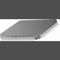
CR16MCS9VJE8 National Semiconductor, CR16MCS9VJE8 Datasheet - Page 52

CR16MCS9VJE8
Manufacturer Part Number
CR16MCS9VJE8
Description
16-Bit Microcontroller IC
Manufacturer
National Semiconductor
Datasheet
1.CR16MCS9VJE8.pdf
(156 pages)
Specifications of CR16MCS9VJE8
Controller Family/series
CR16X
Core Size
16 Bit
Program Memory Size
64K X 8 Flash
Digital Ic Case Style
PQFP
No. Of Pins
80
Mounting Type
Surface Mount
Clock Frequency
25MHz
Lead Free Status / RoHS Status
Contains lead / RoHS non-compliant
Available stocks
Company
Part Number
Manufacturer
Quantity
Price
Company:
Part Number:
CR16MCS9VJE8
Manufacturer:
ON
Quantity:
8 917
Company:
Part Number:
CR16MCS9VJE8-CBB
Manufacturer:
ON
Quantity:
846
Company:
Part Number:
CR16MCS9VJE8-CBC
Manufacturer:
ON
Quantity:
109
Company:
Part Number:
CR16MCS9VJE8-CBD
Manufacturer:
ON
Quantity:
17
Company:
Part Number:
CR16MCS9VJE8-CBE
Manufacturer:
ON
Quantity:
1 950
www.national.com
The TnA and TnB pins function as capture inputs. A transition
received on the TnA pin transfers the timer contents to the
TnCRA register. Similarly, a transition received on the TnB
The TnA and TnB inputs can be configured to preset the
counter to FFFF hex upon reception of a valid capture event.
In this case, the current value of the counter is transferred to
the corresponding capture register and then the counter is
preset to FFFF hex. Using this approach allows the software
to determine the on-time and off-time and period of an exter-
nal signal with a minimum of CPU overhead.
The values captured in the TnCRA register at different times
reflect the elapsed time between transitions on the TnA pin.
The same is true for the TnCRB register and the TnB pin. The
input signal on TnA or TnB must have a pulse width equal to
or greater than one system clock cycle.
There are three separate interrupts associated with the cap-
ture timer, each with its own enable bit and pending flag. The
three interrupt events are reception of a transition on TnA, re-
ception of a transition on TnB, and underflow of the TnCNT1
counter. The enable bits for these events are TnAIEN, TnBI-
EN, and TnCIEN, respectively.
In Mode 2, Timer/Counter II (TnCNT2) can be used as a sim-
ple system timer. The clock counts down using the clock se-
lected with the Timer/Counter II clock selector. It generates
Timer I
Timer II
Clock
Clock
Figure 15. Mode 2: Dual Input Capture Block Diagram
Timer/Counter I
Timer/Counter II
TnCNT1
Capture A
Capture B
TnCRA
TnCRB
TnCNT2
Preset
Preset
Underflow
52
Underflow
pin transfers the timer contents to the TnCRB register. Each
input pin can be configured to sense either rising or falling
edges.
an interrupt upon each underflow if the interrupt is enabled
with the TnDIEN bit.
Neither Timer/Counter I (TnCNT1) nor Timer/Counter II
(TnCNT2) can be configured to operate as an external event
counter or to operate in the pulse accumulate mode because
the TnB input is used as a capture input. Attempting to select
one of these configurations will cause one or both counters
to stop.
15.2.3
Mode 3 is the Dual Independent Timer mode, which gener-
ates system timing signals or counts occurrences of external
events.
Figure16 is a block diagram of the Multi-Function Timer con-
figured to operate in Mode 3. The timer is configured to oper-
ate as a dual independent system timer or dual external
event counter. In addition, Timer/Counter I can generate a
50% duty cycle PWM signal on the TnA pin. The TnB pin can
be used as an external event input or pulse accumulate input
and can be used as the clock source for either Timer/Counter
I or Timer/Counter II. Both counters can also be clocked by
the prescaled system clock.
TnAEN
TnBEN
Mode 3: Dual Independent Timer/Counter
TnCIEN
TnAIEN
TnBIEN
TnDIEN
TnCPND
TnAPND
TnBPND
TnDPND
Interrupt I
Interrupt I
Interrupt I
Interrupt II
Timer
Timer
Timer
Timer
TnB
TnA


