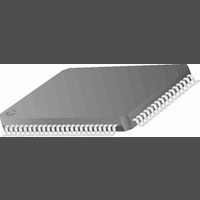
CR16MCS9VJE8 National Semiconductor, CR16MCS9VJE8 Datasheet - Page 154

CR16MCS9VJE8
Manufacturer Part Number
CR16MCS9VJE8
Description
16-Bit Microcontroller IC
Manufacturer
National Semiconductor
Datasheet
1.CR16MCS9VJE8.pdf
(156 pages)
Specifications of CR16MCS9VJE8
Controller Family/series
CR16X
Core Size
16 Bit
Program Memory Size
64K X 8 Flash
Digital Ic Case Style
PQFP
No. Of Pins
80
Mounting Type
Surface Mount
Clock Frequency
25MHz
Lead Free Status / RoHS Status
Contains lead / RoHS non-compliant
Available stocks
Company
Part Number
Manufacturer
Quantity
Price
Company:
Part Number:
CR16MCS9VJE8
Manufacturer:
ON
Quantity:
8 917
Company:
Part Number:
CR16MCS9VJE8-CBB
Manufacturer:
ON
Quantity:
846
Company:
Part Number:
CR16MCS9VJE8-CBC
Manufacturer:
ON
Quantity:
109
Company:
Part Number:
CR16MCS9VJE8-CBD
Manufacturer:
ON
Quantity:
17
Company:
Part Number:
CR16MCS9VJE8-CBE
Manufacturer:
ON
Quantity:
1 950
www.national.com
When a frame was successfully sent by CR16CAN the con-
tents of the Time Stamp counter are captured into the Time
Stamp register (TSTP) of the transmit buffer during the ACK-
slot of the frame currently being sent. Also, when a message
is received, the TSTP-register of the receiving buffer is load-
ed with the Time Stamp counter value during the ACK-slot of
the CAN frame currently being received.
This means, in the case where a message is received in one
buffer, which was sent from another buffer of the same
CR16CAN node, the TSTP-register contents are equal after
this transaction.
A comparison of the two TSTP-register values can be insert-
ed into a "read from CAN receive buffer" software routine, to
distinguish whether the data received are from another CAN
node (valid) or from the same CAN node (invalid).
The flowchart below shows a possible implementation. The
same CAN buffer settings as described in Section also apply
to this example.
Modified CAN Receive Sequence:
Advantage:
None of the CAN receive buffers must be disabled at any
time.
Disadvantage:
The receive buffer contents are overwritten by an invalid
message sent from the same CR16CAN node.
Reset Buffer 1 Status to
Read out Buffer 1 Data
Message received
Time Stamp of
Time Stamp of
into Buffer 1
RX_READY
Buffer 1
Buffer 0
Exit
=
154
26.2
26.2.1
According to the specification, the MSKn clock output in mas-
ter mode should have the value of the MnIDL bit of the
MWnCTL register, even when the module is disabled. How-
ever, the MSKn pin is enabled and the module is disabled.
thus, even if the MnIDL bit is set, the MSKn clock will change
to a low level as soon as the module is disabled. If any slave
is selected at this time, i will interpret this unwanted transition
as a shift clock.
26.2.2
Even if the module is disabled and the alternate function of
the MSKn pin is enabled, the module can still influence the
MSKn pin and drives the default value ‘0’.
26.2.3
When the MSKn idle level of ‘1’ is to be used, the following
procedure should be followed when the module is disabled:
26.3
26.3.1
The available window for a valid WATCHDOG service varies
with the TWM configuration and the operating mode of the
R16MCS9. Therefore it is not possible to generally provide
the limits for the maximum service window. However, the lim-
its for the minimum service window is guaranteed and should
be used.
26.3.2
The timing and WATCHDOG module uses two different clock
signals for its operation, the slow system clock as well as the
fast system clock.
The slow system clock can either be generated by an exter-
nal 32 kHz quartz or it can be derived from the fast system
clock by means of a prescaler counter in the CLK2RES mod-
ules. The TWM can operate off a maximum slow system
clock of 100 kHz. The WATCHDOG counter (down-counter)
is either clocked directly by the slow system (T0IN) or it is
decremented every time the counter T0 underflows
(T0OUT).
The fast system clock is used for accesses to TWM registers,
which build the user interface of the TWM. These user inter-
face registers include all memory-mapped registers of the
TWM.
1. Set the MSKn pin to high level in the corresponding port
2. Configure the MSKn pin to an output in the correspond-
3. Disable the alternate function of the MSKn pin in the cor-
4. Disable the MWSPI16 module.
data output register.
ing port direction register.
responding port alternate function register.
8/16-BIT MICROWIRE/SPI (MWSPI16)
MWSPI16 Problem Description
MWSPI16 Problem Cause
MWSPI16 Problem Solutions
TIMING AND WATCHDOG MODULE
Timing and WATCHDOG Module Problem
Description
Timing and WATCHDOG Module Problem
Cause


