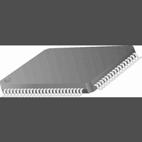
CR16MCS9VJE8 National Semiconductor, CR16MCS9VJE8 Datasheet - Page 12

CR16MCS9VJE8
Manufacturer Part Number
CR16MCS9VJE8
Description
16-Bit Microcontroller IC
Manufacturer
National Semiconductor
Datasheet
1.CR16MCS9VJE8.pdf
(156 pages)
Specifications of CR16MCS9VJE8
Controller Family/series
CR16X
Core Size
16 Bit
Program Memory Size
64K X 8 Flash
Digital Ic Case Style
PQFP
No. Of Pins
80
Mounting Type
Surface Mount
Clock Frequency
25MHz
Lead Free Status / RoHS Status
Contains lead / RoHS non-compliant
Available stocks
Company
Part Number
Manufacturer
Quantity
Price
Company:
Part Number:
CR16MCS9VJE8
Manufacturer:
ON
Quantity:
8 917
Company:
Part Number:
CR16MCS9VJE8-CBB
Manufacturer:
ON
Quantity:
846
Company:
Part Number:
CR16MCS9VJE8-CBC
Manufacturer:
ON
Quantity:
109
Company:
Part Number:
CR16MCS9VJE8-CBD
Manufacturer:
ON
Quantity:
17
Company:
Part Number:
CR16MCS9VJE8-CBE
Manufacturer:
ON
Quantity:
1 950
www.national.com
5.0
The device has two input pins, ENV0 and ENV1, which are
used to specify the operating environment of the device upon
reset. There are also two system configuration registers,
called the Module Configuration (MCFG) register and the
Module Status (MSTAT) register.
5.1
Upon reset, the operating mode of the device is determined
by the state of the ENV0 and ENV1 input pins, as indicated
in Table6.
In the case where the ENV1 and ENV0 pins are both high,
the reset algorithm looks at the FLCTRL2.EMPTY bit to de-
termine whether the program memory is empty, and sets the
operating mode accordingly.
The ENV0 and ENV1 pins have on-chip pull-up devices that
are enabled during reset while the pins are being sampled.
Therefore, if they are left unconnected, the inputs are consid-
ered high and the normal operating mode (IRE-Mode) is se-
lected and the CPU starts to execute code at address 0. To
enter any other operating mode, the external hardware must
drive the appropriate input low.
In the case where the ISP-Mode is selected, the chip starts
executing the ISP code residing in the on-chip ISP-Memory
area.
The test modes are Reserved for factory testing and for ex-
ternal programming of the flash EEPROM program memory.
They should not be invoked otherwise.
5.2
The MCFG register is a byte-wide, read/write register that
sets the clock output features of the device.
Upon reset, the non-reserved bits of this register are cleared
to zero. The start-up software must write a specific value to
this register in order to configure the CLK output pin function.
When the software writes to this register, it must write a zero
to each reserved bit for the device to operate properly. The
register should be written in active mode only, not in power
save, HALT, or IDLE mode. However, the register contents
are preserved during all power modes.
The MCFG register format is shown below.
CLKOE
Reserved CLK2OE
ENV1
7
0
0
1
1
6
Table 6 Operating Environment Selection
System Configuration
ENV0 AND ENV1 PINS
MODULE CONFIGURATION (MCFG)
REGISTER
ENV0
5
0
1
0
1
CPU Clock Output Enable. When this bit is
cleared (0), the CLK pin (ENV1) remains in the
high-impedance state. When this bit is set (1) in
Test Mode Flash Memory
Test Mode
In-System-Programming mode (ISP)
Internal ROM enabled Mode (IRE), if
program memory is not empty; or ISP-
Mode, if program memory is empty
4
Reserved
Operating Environment
3
CLK1OE
2
CLKOE Reserved
1
0
12
CLK1OE
CLK2OE
5.3
The MSTAT register is a byte-wide, read-only register that in-
dicates the general status of the device.
The MCFG register format is shown below.
OENV(1:0)
PGMBUSY Flash EEPROM Programming Busy. This bit is
7
Reserved
MODULE STATUS (MSTAT) REGISTER
4
normal operating mode, the CLK pin operates
as a CPU clock output.
Generated Clock Output 1 Enable. When
cleared (0), the CLKOUT1 pin (ENV0) stays in
high impedance state. When set (1), the pin
outputs the clock from the prescaler controlled
by PRSSC1.SCDIV1.
Generated Clock Output 2 Enable. When this
bit is set (1) and CLKOE is cleared, the
CLKOUT2 pin (ENV1) outputs the clock from
the prescaler controlled by PRSSC1.SCDIV2.
Otherwise, the CLKOUT2 pin is in high imped-
ance state.
Operating Environment. These two bits contain
the values applied to the ENV1 and ENV0 pins
upon reset. These bit values are controlled by
the external hardware upon reset and are held
constant in the register until the next reset.
automatically set to 1 when either the program
memory or the data memory is busy being pro-
grammed or erased. It is cleared to 0 when nei-
ther of the two flash EEPROM memories is
busy being programmed or erased. When this
bit is set, the software should not attempt any
write access to either of these two memories.
PGMBUSY
3
Reserved
2
OENV1
1
OENV0
0


