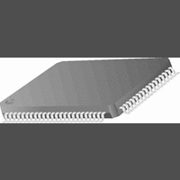
CR16MCS9VJE8 National Semiconductor, CR16MCS9VJE8 Datasheet - Page 20

CR16MCS9VJE8
Manufacturer Part Number
CR16MCS9VJE8
Description
16-Bit Microcontroller IC
Manufacturer
National Semiconductor
Datasheet
1.CR16MCS9VJE8.pdf
(156 pages)
Specifications of CR16MCS9VJE8
Controller Family/series
CR16X
Core Size
16 Bit
Program Memory Size
64K X 8 Flash
Digital Ic Case Style
PQFP
No. Of Pins
80
Mounting Type
Surface Mount
Clock Frequency
25MHz
Lead Free Status / RoHS Status
Contains lead / RoHS non-compliant
Available stocks
Company
Part Number
Manufacturer
Quantity
Price
Company:
Part Number:
CR16MCS9VJE8
Manufacturer:
ON
Quantity:
8 917
Company:
Part Number:
CR16MCS9VJE8-CBB
Manufacturer:
ON
Quantity:
846
Company:
Part Number:
CR16MCS9VJE8-CBC
Manufacturer:
ON
Quantity:
109
Company:
Part Number:
CR16MCS9VJE8-CBD
Manufacturer:
ON
Quantity:
17
Company:
Part Number:
CR16MCS9VJE8-CBE
Manufacturer:
ON
Quantity:
1 950
www.national.com
BW
FRE
IPST
IPRE
Note: Reserved bits must be cleared to 0 when the CPU
writes to the register.
8.3
The number of wait cycles and hold cycles inserted into a bus
cycle depends on whether it is a read or write operation, the
type of memory or I/O being accessed, and the control regis-
ter settings.
8.3.1
When the CPU accesses the flash EEPROM program mem-
ory (address ranges 0000-BFFF and 1C000-1FFFF), the
number of added wait and hold cycles depends on the type
of access and the BIU register settings.
In fast read mode (SZCFG0.FRE=1), a read operation is a
single cycle access. This limits the maximum CPU operating
frequency to either 10 MHz or 20 MHz (see Section9.1.5).
For a read operation in normal read mode (SZCFG0.FRE=0),
the number of inserted wait cycles is one plus the value writ-
ten to the SZCFG0.WAIT field. The number in this field can
range from zero to seven, so the total number of wait cycles
can range from one to eight. The number of inserted hold cy-
cles is equal to the value written to the SCCFG0.HOLD field,
which can range from zero to three.
For a write operation in fast read mode (SZCFG0.FRE=1),
the number of inserted wait cycles is one. No hold cycles are
used.
Flash EEPROM Program Memory
WAIT AND HOLD STATES USED
cycles used for each memory access, ranging
from 00 binary for no T hold cycles to 11 binary
for three T hold clock cycles. These bits are ig-
nored if the SZCFG0.FRE bit is set to 1.
Bus Width.
This bit defines the bus width of the zone.
If cleared to 0, a bus width of 8-bit is used.
if set to 1, a bus width of 16-bit is used.
For the device a bus width of 16-bit needs to be
set.
Fast Read Enable
This bit enables (1) or disables (0) fast read bus
cycles. A fast read operation takes one clock
cycle. A normal read operation takes at least
two clock cycles.
Post Idle.
An idle cycle follows the current bus cycle,
when the next bus cycle accesses a different
zone.
If cleared to 0, no idle cycle is inserted.
If set to 1, one idle cycle is inserted.
The IPST bit can be cleared to 0, as no idle cy-
cles are required for on-chip accesses.
Preliminary Idle.
An idle cycle is inserted prior to the current bus
cycle, when the new bus cycle accesses a dif-
ferent zone.
If cleared to 0, no idle cycle is inserted.
If set to 1, one idle cycle is inserted.
The IPRE bit can be cleared to 0, as no idle cy-
cles are required for on-chip accesses.
20
For a write operation normal read mode (SZCFG0.FRE=0),
the number of wait cycles is equal to the value written to the
SZCFG0. WAIT field plus one (in the late write mode) or two
(in the early write mode). The number of inserted hold cycles
is equal to the value written to the SCCFG0.HOLD field,
which can range from zero to three.
Writing to the flash EEPROM program memory is a Flash
programming operation that requires some additional steps,
as explained in Section9.3.
8.3.2
Read and write accesses to on-chip RAM is performed within
a single cycle, regardless of the BIU settings.
8.3.3
There is either no wait state or one wait state used when the
CPU accesses the EEPROM data memory (address F000-
F27F hex). The number of required wait states (zero or one)
depends on the CPU clock frequency and operating mode,
and is controlled by programming of the DMCSR.ZEROWS
bit in the MCFG register, as explained in Section9.3. No hold
cycles are used.
8.3.4
When the CPU accesses on-chip peripherals in the range of
F800-FAFF hex and FC00-FFFF hex, one wait cycle and one
preliminary idle cycle is used. No hold cycles are used.
The IOCFG register determines the access timing for the ad-
dress range FB00-FB16 hex (Ports B and Port C).
RAM Memory
EEPROM Data Memory
Accesses to Peripheral


