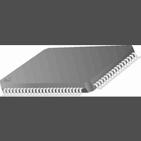
CR16MCS9VJE8 National Semiconductor, CR16MCS9VJE8 Datasheet - Page 136

CR16MCS9VJE8
Manufacturer Part Number
CR16MCS9VJE8
Description
16-Bit Microcontroller IC
Manufacturer
National Semiconductor
Datasheet
1.CR16MCS9VJE8.pdf
(156 pages)
Specifications of CR16MCS9VJE8
Controller Family/series
CR16X
Core Size
16 Bit
Program Memory Size
64K X 8 Flash
Digital Ic Case Style
PQFP
No. Of Pins
80
Mounting Type
Surface Mount
Clock Frequency
25MHz
Lead Free Status / RoHS Status
Contains lead / RoHS non-compliant
Available stocks
Company
Part Number
Manufacturer
Quantity
Price
Company:
Part Number:
CR16MCS9VJE8
Manufacturer:
ON
Quantity:
8 917
Company:
Part Number:
CR16MCS9VJE8-CBB
Manufacturer:
ON
Quantity:
846
Company:
Part Number:
CR16MCS9VJE8-CBC
Manufacturer:
ON
Quantity:
109
Company:
Part Number:
CR16MCS9VJE8-CBD
Manufacturer:
ON
Quantity:
17
Company:
Part Number:
CR16MCS9VJE8-CBE
Manufacturer:
ON
Quantity:
1 950
www.national.com
25.0 ELECTRICAL AND THERMAL CHARACTERISTICS
Absolute Maximum Ratings
If Military/Aerospace specified devices are required, please
contact the National Semiconductor Sales Office/Distributors
for availability and specifications.
Thermal Characteristics
DC Electrical Characteristics:
Supply Voltage (V
Voltage at Any Pin *
ESD Protection Level
Total Current into V
Average junction temperature
Ambient temperature
Package thermal resistance (junction-to-ambient)
Total power dissipation
Device internal power
dissipation
I/O pin power dissipation
A constant
1. This is an approximate value, neglecting P
2. For most applications P
3. K is a constant pertaining to the device. Solve for K with a known T
P
V
V
V
V
Vxl
Vxh
Vxl2
Vxh2
V
I
I
Symbol
80-pin quad flat pack (QFP)
OH
O L
D
IH
IL
IHACB
ILACB
hys
and T
J
iterntively for any value of T
3
Operating Voltage
Logical 1 CMOS Input Voltage (except ACB & clocks)
Logical 0 CMOS Input Voltage (except ACB & clocks)
SDA, SCL Logical 1 CMOS Input Voltage
SDA, SCL Logical 0 CMOS Input Voltage
Low Level Input Voltage OSC
High Level Input Voltage OSC
X2CKI Logical 0 Input Voltage
X2CKI Logical 1 Input Voltage
Hysteresis Loop Width
Logical 1 CMOS Output Current
Logical 0 CMOS Output Current
CC
CC
)
Characteristics
Pin (Source)
1
I/O
2
<<
P
INT
and can be neglected.
Parameter
A
a
.
(Human Body Model)
–0.6V to V
I/O
.
–40°C
CC
200 mA
TA +85°C (also supports -40°C to +125°C)
+0.6V
2 kV
7V
136
A
and a measured P
Note: Absolute maximum ratings indicate limits beyond
which damage to the device may occur. DC and AC electrical
specifications are not ensured when operating the device at
absolute maximum ratings. * The latch-up tolerance on Ac-
cess Bus pins 14 and 15 exceeds 150mA.
Total Current out of GND Pin (Sink)
Storage Temperature Range
Symbol
External X1 clock
External X1 clock
External X2 clock
External X2clock
V
V
P
P
~
P
T
T
OH
OL
INT
K
JA
I/O
A
D
J
= 0.45V, Vcc=4.5V
= 3.8V, Vcc=4.5V
Conditions
D
(at equilibrium). Use this value of K to solve for
P
User-determined
User-determined
D
T
A
x (T
T
P
I
~
+ (P
DD
J
INT
JA
Value
A
+ 273°C
49.8
X V
or
K
+ 273°C) +
D
+ P
x P
0.8Vcc
0.7Vcc
0.5Vcc
0.1Vcc
X ~
-0.5
-1.6
4.5
1.2
1.6
Min
DD
D
0
I/O
2
JA
)
Vcc + 0.5
–65°C to +150°C
0.2Vcc
0.3Vcc
0.2Vcc
Max
Vcc
5.5
0.3
W, °C
°C/W
200 mA
Unit
°C
°C
W
W
W
Units
mA
mA
V
V
V
V
V
V
V
V
V
V


