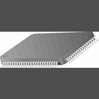
CR16MCS9VJE8 National Semiconductor, CR16MCS9VJE8 Datasheet - Page 19

CR16MCS9VJE8
Manufacturer Part Number
CR16MCS9VJE8
Description
16-Bit Microcontroller IC
Manufacturer
National Semiconductor
Datasheet
1.CR16MCS9VJE8.pdf
(156 pages)
Specifications of CR16MCS9VJE8
Controller Family/series
CR16X
Core Size
16 Bit
Program Memory Size
64K X 8 Flash
Digital Ic Case Style
PQFP
No. Of Pins
80
Mounting Type
Surface Mount
Clock Frequency
25MHz
Lead Free Status / RoHS Status
Contains lead / RoHS non-compliant
Available stocks
Company
Part Number
Manufacturer
Quantity
Price
Company:
Part Number:
CR16MCS9VJE8
Manufacturer:
ON
Quantity:
8 917
Company:
Part Number:
CR16MCS9VJE8-CBB
Manufacturer:
ON
Quantity:
846
Company:
Part Number:
CR16MCS9VJE8-CBC
Manufacturer:
ON
Quantity:
109
Company:
Part Number:
CR16MCS9VJE8-CBD
Manufacturer:
ON
Quantity:
17
Company:
Part Number:
CR16MCS9VJE8-CBE
Manufacturer:
ON
Quantity:
1 950
The IOCFG register address is F902 hex. Upon reset, the
register is initialized to 069F hex. The register format is
shown below.
WAIT
HOLD
BW
IPST
Note: Reserved bits must be cleared to 0 when the CPU
writes to the register.
8.2.3
The Static Zone 0 Configuration (SZCFG0) register is a
word-wide, read/write register that sets the timing and bus
characteristics of Zone 0 memory accesses. In the device im-
plementation of the CompactRISC architecture, Zone 0 is oc-
cupied by the flash EEPROM program memory.
The SCCFG0 register address is F904 hex. Upon reset, the
register is initialized to 069F hex. The register format is
shown below.
WAIT
15 14 13 12
15 14 13 12
BW
BW
7
7
Reserved
Static Zone 0 Configuration (SZCFG0) Register
Reserved
Reserved
6
6
Reserved
Memory Wait cycles
This field specifies the number of TIW (internal
wait state) clock cycles added for each memory
access, ranging from 000 binary for no addi-
tional TIW wait cycles to 111 binary for seven
additional TIW wait cycles.
Memory Hold cycles
This field specifies the number of T hold clock
cycles used for each memory access, ranging
from 00 binary for no T hold cycles to 11 binary
for three T hold clock cycles.
Bus Width.
This bit defines the bus width of the zone.
If cleared to 0, a bus width of 8-bit is used.
if set to 1, a bus width of 16-bit is used.
For the device, a bus width of 16-bit needs to
be set.
Post Idle.
An idle cycle follows the current bus cycle,
when the next bus cycle accesses a different
zone.
If cleared to 0, no idle cycle is inserted.
If set to 1, one idle cycle is inserted.
The IPST bit can be cleared to 0, as no idle cy-
cles are required for on-chip accesses.
Memory Wait cycles
This field specifies the number of TIW (internal
wait state) clock cycles added for each memory
access, ranging from 000 binary for no addi-
tional TIW wait cycles to 111 binary for seven
additional TIW wait cycles. These bits are ig-
nored if the SZCFG0.FRE bit is set to 1.
5
5
FRE
11
11
4
4
HOLD
HOLD
IPRE
10
10
3
3
IPST
IPST
9
2
9
2
WAIT
WAIT
Reserved
1
Reserved
1
8
8
0
0
19
HOLD
BW
FRE
IPST
IPRE
Note: Reserved bits must be cleared to 0 when the CPU
writes to the register.
8.2.4
The Static Zone 1 Configuration (SZCFG1) register is a
word-wide, read/write register that sets the timing and bus
characteristics of Zone 1 memory accesses. In the device im-
plementation of the CompactRISC architecture, Zone 1 is oc-
cupied by the boot ROM memory (ISP-Memory).
The SCCFG1 register address is F906 hex. Upon reset, the
register is initialized to 069F hex. The register format is
shown below.
WAIT
HOLD
15 14 13 12
BW
7
Reserved
Static Zone 1 Configuration (SZCFG1) Register
Reserved
6
Memory Hold cycles
This field specifies the number of T hold clock
cycles used for each memory access, ranging
from 00 binary for no T hold cycles to 11 binary
for three T hold clock cycles. These bits are ig-
nored if the SZCFG0.FRE bit is set to 1.
Bus Width.
This bit defines the bus width of the zone.
If cleared to 0, a bus width of 8-bit is used.
if set to 1, a bus width of 16-bit is used.
For the devicedevice a bus width of 16-bit
needs to be set.
Fast Read Enable
This bit enables (1) or disables (0) fast read
bus cycles. A fast read operation takes one
clock cycle. A normal read operation takes at
least two clock cycles.
Post Idle.
An idle cycle follows the current bus cycle,
when the next bus cycle accesses a different
zone.
If cleared to 0, no idle cycle is inserted.
If set to 1, one idle cycle is inserted.
The IPST bit can be cleared to 0, as no idle cy-
cles are required for on-chip accesses.
Preliminary Idle.
An idle cycle is inserted prior to the current bus
cycle, when the new bus cycle accesses a dif-
ferent zone.
If cleared to 0, no idle cycle is inserted.
If set to 1, one idle cycle is inserted.
The IPRE bit can be cleared to 0, as no idle cy-
cles are required for on-chip accesses.
Memory Wait cycles
This field specifies the number of TIW (internal
wait state) clock cycles added for each memory
access, ranging from 000 binary for no addi-
tional TIW wait cycles to 111 binary for seven
additional TIW wait cycles. These bits are ig-
nored if the SZCFG0.FRE bit is set to 1.
Memory Hold cycles
This field specifies the number of T hold clock
5
FRE
11
4
HOLD
IPRE
10
3
IPST
9
2
www.national.com
WAIT
Reserved
1
8
0


