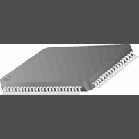
CR16MCS9VJE8 National Semiconductor, CR16MCS9VJE8 Datasheet - Page 79

CR16MCS9VJE8
Manufacturer Part Number
CR16MCS9VJE8
Description
16-Bit Microcontroller IC
Manufacturer
National Semiconductor
Datasheet
1.CR16MCS9VJE8.pdf
(156 pages)
Specifications of CR16MCS9VJE8
Controller Family/series
CR16X
Core Size
16 Bit
Program Memory Size
64K X 8 Flash
Digital Ic Case Style
PQFP
No. Of Pins
80
Mounting Type
Surface Mount
Clock Frequency
25MHz
Lead Free Status / RoHS Status
Contains lead / RoHS non-compliant
Available stocks
Company
Part Number
Manufacturer
Quantity
Price
Company:
Part Number:
CR16MCS9VJE8
Manufacturer:
ON
Quantity:
8 917
Company:
Part Number:
CR16MCS9VJE8-CBB
Manufacturer:
ON
Quantity:
846
Company:
Part Number:
CR16MCS9VJE8-CBC
Manufacturer:
ON
Quantity:
109
Company:
Part Number:
CR16MCS9VJE8-CBD
Manufacturer:
ON
Quantity:
17
Company:
Part Number:
CR16MCS9VJE8-CBE
Manufacturer:
ON
Quantity:
1 950
transferred, and the acknowledge signal sent by the receiv-
ing device (Figure 41).
The master generates the acknowledge clock pulse on the
ninth clock pulse of the byte transfer. The transmitter releas-
es the SDA line (permits it to go high) to allow the receiver to
send the acknowledge signal. The receiver must pull down
the SDA line during the acknowledge clock pulse, thus sig-
nalling the correct reception of the last data byte, and its
readiness to receive the next byte. Figure 42 illustrates the
acknowledge cycle.
The master generates an acknowledge clock pulse after
each byte transfer. The receiver sends an acknowledge sig-
nal after every byte received.
There are two exceptions to the “acknowledge after every
byte” rule.
Addressing Transfer Formats
Each device on the bus has a unique address. Before any
data is transmitted, the master transmits the address of the
slave being addressed. The slave device should send an ac-
knowledge signal on the SDA line, once it recognizes its ad-
dress.
1. When the master is the receiver, it must indicate to the
2. When the receiver is full, otherwise occupied, or a prob-
SDA
SCL
Data Output
Data Output
Transmitter
Receiver
transmitter an end of data by not-acknowledging (“neg-
ative acknowledge”) the last byte clocked out of the
slave. This “negative acknowledge” still includes the ac-
knowledge clock pulse (generated by the master), but
the SDA line is not pulled down.
lem has occurred, it sends a negative acknowledge to
indicate that it can not accept additional data bytes.
Start
Condition
by
by
Figure 42. ACCESS.bus Acknowledge Cycle
S
Figure 41.
SCL
MSB
1
Start
Condition
S
2 3 - 6
I
Byte Complete
nterrupt Within
ACCESS.bus Data Transaction
1
7
Receiver
2 3 - 6
8
ACK
9
Acknowledgment
Signal From Receiver
7
1
Clock Line Held
Low by Receiver
While Interrupt
is Serviced
8
2
Transmitter Stays Off
the Bus During the
Acknowledgment Clock
9
Acknowledgment
Signal From Receiver
3 - 8
ACK
9
Condition
Stop
P
79
The address is the first seven bits after a Start Condition. The
direction of the data transfer (R/W) depends on the bit sent
after the address — the eighth bit. A low-to-high transition
during a SCL high period indicates the Stop Condition, and
ends the transaction (Figure 43).
SDA
SCL
When the address is sent, each device in the system com-
pares this address with its own. If there is a match, the device
considers itself addressed and sends an acknowledge sig-
nal. Depending upon the state of the R/W bit (1:read,
0:write), the device acts as a transmitter or a receiver.
The I
to all slaves connected to the bus. The first byte sent speci-
fies the general call address (00
specifies the meaning of the general call (for example, “Write
slave address by software only”). Those slaves that require
the data acknowledge the call and become slave receivers;
the other slaves ignore the call.
Arbitration on the Bus
Multiple master devices on the bus, require arbitration be-
tween their conflicting bus-access demands. Control of the
bus is initially determined according to address bits and clock
cycle. If the masters are trying to address the same IC, data
comparisons determine the outcome of this arbitration. In
master mode, the device immediately aborts a transaction if
the value sampled on the SDA lines differs from the value
driven by the device. (Exceptions to this rule are SDA while
receiving data; in these cases the lines may be driven low by
the slave without causing an abort).
The SCL signal is monitored for clock synchronization pur-
pose and allow the slave to stall the bus. The actual clock pe-
riod will be the one set by the master with the longest clock
period or by the slave stall period. The clock high period is
determined by the master with the shortest clock high period.
When an abort occurs during the address transmission, the
master that identify the conflict, give-up the bus and should
switch to slave mode and continue to sample SDA to see if it
is being addressed by the winning master on the AC-
CESS.bus.
19.2
The ACB module provides the physical layer for an AC-
CESS.bus compliant serial interface. The module is config-
urable as either a master or slave device. As a slave device,
the ACB module may issue a request to become the bus
master.
Figure 43. A Complete ACCESS.bus Data Transaction
Start
Condition
2
C bus protocol allows sending a general call address
S
ACB FUNCTIONAL DESCRIPTION
Address R/ W ACK
1 - 7
8
9
1 - 7
Data
8
16
ACK
) and the second byte
9
1 - 7
www.national.com
Data
8
ACK
9
Stop
Condition
P


