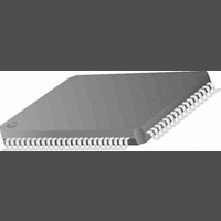
CR16MCS9VJE8 National Semiconductor, CR16MCS9VJE8 Datasheet - Page 116

CR16MCS9VJE8
Manufacturer Part Number
CR16MCS9VJE8
Description
16-Bit Microcontroller IC
Manufacturer
National Semiconductor
Datasheet
1.CR16MCS9VJE8.pdf
(156 pages)
Specifications of CR16MCS9VJE8
Controller Family/series
CR16X
Core Size
16 Bit
Program Memory Size
64K X 8 Flash
Digital Ic Case Style
PQFP
No. Of Pins
80
Mounting Type
Surface Mount
Clock Frequency
25MHz
Lead Free Status / RoHS Status
Contains lead / RoHS non-compliant
Available stocks
Company
Part Number
Manufacturer
Quantity
Price
Company:
Part Number:
CR16MCS9VJE8
Manufacturer:
ON
Quantity:
8 917
Company:
Part Number:
CR16MCS9VJE8-CBB
Manufacturer:
ON
Quantity:
846
Company:
Part Number:
CR16MCS9VJE8-CBC
Manufacturer:
ON
Quantity:
109
Company:
Part Number:
CR16MCS9VJE8-CBD
Manufacturer:
ON
Quantity:
17
Company:
Part Number:
CR16MCS9VJE8-CBE
Manufacturer:
ON
Quantity:
1 950
www.national.com
20.9.19 CAN Timer Register (CTMR)
The current value of the Time Stamp counter as described in
section 20.8 can be monitored via the CAN Timer Register.
The CAN Time register is a free running 16-bit counter. It con-
tains the number of CAN bits recognized by CR16CAN since
the register has been reset. The counter starts to increment
from the value 0000
Stamp enable flag (TSTPEN) in the CAN global configuration
register (CGCR) is set, the counter will also be reset upon a
message transfer of the message buffer 0.
As described in Time Stamp Counter on page 105, the con-
tents of CTMR are captured into the Time Stamp register of
the message buffer after successfully sending or receiving a
frame.
20.10
After system start-up, all CR16CAN related registers are in
their reset state. The CR16CAN module can be enabled after
all configuration registers are set to their desired value. The
following initial setting need to be made:
Before disabling the CR16CAN module, the user has to
make sure that no transmission is still pending.
Note: The device can be awaken from a power saving mode
by an activity on the CAN bus by selecting the CAN RX pin
as an input to the Multi-Input Wake-Up module. In this case
the CR16CAN module must not be disabled before entering
the power saving mode. Disabling the CR16CAN module
also disables the CAN RX pin.
As an alternative, the CAN RX pin can be connected to any
other input pin of the Multi-Input Wake-Up module. This input
channel must then be configured to trigger a wake-up event
on a falling edge (if a dominant bit is represented by a low lev-
el). In this case the CR16CAN module can be disabled be-
fore entering a power saving mode. After the device has
been waken up, the user has to manually enable the
CR16CAN again. All configuration and buffer registers still
contain the same data as prior to the power down phase.
20.10.1 External Connection
The CR16CAN uses two external pins, CANTX and CANRX
to connect to the physical layer of the CAN interface. They
provide the functionality as described in Table38.
— configure the CAN Timing register (CTIM) See “ B it
— configure every buffer to its function as receive/trans-
— set the acceptance filtering masks. See “Acceptance
— enable the CR16CAN interface. See “ C AN Global
15
Time Logic” on page94.
mit Buffer Status/Control Register (CNSTAT) on page
106.
Filtering” on page96.
Configuration Register (CGCR)” on page109.
SYSTEM START-UP AND MULTI-INPUT
WAKE-UP
receiver will not drive the bus except during
ACK and during an active error flag.
16
after a hardware reset. If the Timer
CTMR[15:0]
0
r
0
116
The logic levels are configurable by means of two control
flags CTX and CRX of the Global Configuration Register
CGCR (see “CAN Global Configuration Register (CGCR) ” on
page 109.
20.10.2 Transceiver Connection
An external Transceiver Chip needs to be connected be-
tween the CAN block and the bus. It is used to establish a bus
connection in differential mode and furthermore provides the
driver and protection requirements.
20.10.3 Timing Requirements
Processing messages and updating message buffers require
a certain number of clock cycles by CR16CAN as shown in
Table39. These requirements may lead to some restrictions
regarding the Bit Time Logic settings and the overall
CR16CAN performance which are described below in more
detail.
CORE BUS
Figure72 shows a possible ISO-High-Speed configuration
Signal Name
schedule a message for trans-
CR16CAN
copy hidden buffer to receive
update status from TX_RTR
Figure 72.
CANRX
CANTX
a. Wait cycles need to be added for CPU access to
b. Depends on the number of matching identifiers.
to TX_ONCE_RTR
CANRX
CANTX
the message memory as described in CPU
Access to CR16CAN Registers/Memory on
page 105.
message buffer
Table 39 CR16CAN Internal Timing
Table 38 External CR16CAN Pins
mission
task
5
4
1
External Transceiver Connection
Output
Transceiver Chip
RX
TX
REF
(ISO-High-Speed)
Type
Input
GND
RS GND
8
BUS_H
BUS_L
GND
2
VCC
Receive data from the CAN bus
Transmit data to the CAN bus
3
7
6
# cycles
Description
VCC
17
3
2
120
a
120
occurrence/
to other modules
termination
CAN Bus Line
frame
0-15
0-1
0-1
b
.


