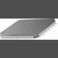
CR16MCS9VJE8 National Semiconductor, CR16MCS9VJE8 Datasheet - Page 105

CR16MCS9VJE8
Manufacturer Part Number
CR16MCS9VJE8
Description
16-Bit Microcontroller IC
Manufacturer
National Semiconductor
Datasheet
1.CR16MCS9VJE8.pdf
(156 pages)
Specifications of CR16MCS9VJE8
Controller Family/series
CR16X
Core Size
16 Bit
Program Memory Size
64K X 8 Flash
Digital Ic Case Style
PQFP
No. Of Pins
80
Mounting Type
Surface Mount
Clock Frequency
25MHz
Lead Free Status / RoHS Status
Contains lead / RoHS non-compliant
Available stocks
Company
Part Number
Manufacturer
Quantity
Price
Company:
Part Number:
CR16MCS9VJE8
Manufacturer:
ON
Quantity:
8 917
Company:
Part Number:
CR16MCS9VJE8-CBB
Manufacturer:
ON
Quantity:
846
Company:
Part Number:
CR16MCS9VJE8-CBC
Manufacturer:
ON
Quantity:
109
Company:
Part Number:
CR16MCS9VJE8-CBD
Manufacturer:
ON
Quantity:
17
Company:
Part Number:
CR16MCS9VJE8-CBE
Manufacturer:
ON
Quantity:
1 950
20.7.2
The interrupt code IST[3:0] can be used within the interrupt
handler as a displacement in order to jump to the relevant
subroutine.
The CAN Interrupt Code Enable (CICEN) register is used in
the CAN interrupt handler if the user wants to service all re-
ceive buffer interrupts first followed by all transmit buffer in-
terrupts. In this case, the user can first enable only all receive
buffer interrupts to be coded, scan and service all pending in-
terrupt requests in the order of their priority. Then, the user
changes the CICEN register to disable all receive buffers, but
enable all transmit buffers and service all pending transmit
buffer interrupt requests according to their priorities.
20.8
CR16CAN features a free running 16-bit timer (CTMR) incre-
menting every bit time recognized on the CAN bus. The val-
ue of this timer during the ACK slot is captured into the TSTP
register of a message buffer after a successful transmission
or reception of a message. Figure68 shows a simplified
block diagram of the Time Stamp counter.
The timer can be synchronized over the CAN network by re-
ceiving or transmitting a message to/from buffer 0. In that
case the TSTP register of buffer 0 captures the current
CTMR value during the ACK slot of a message (as above)
and afterwards the CTMR is reset to 0000
can be enabled or disabled via the CGCR.TSTPEN bit.
ADDR
xxxE
xxxC
xxxA
xxx8
xxx6
xxx4
xxx2
xxx0
16-bit counter
16
16
16
1 6
1 6
1 6
1 6
1 6
TSTP register
Usage Hints
TIME STAMP COUNTER
BUFFER
register
CNTSTAT
DATA0
DATA1
DATA2
DATA3
Figure 68.
TSTP
ID1
ID0
Reset
TSTP15
+1
DLC3
XI28
ID10
XI14
Data
Data
Data
Data
15
1.7
3.7
5.7
7.7
Time Stamp Counter
TSTP14
DLC2
XI27
XI13
Data
Data
Data
Data
14
ID9
1.6
3.6
5.6
7.6
TSTP13 TSTP12
DLC1
ACK slot & buffer 0 active
ACK slot
XI26
XI12
Data
Data
Data
Data
CAN bits on the bus
13
ID8
1.5
3.5
5.5
7.5
Table 25 Message Buffer Organization
2
. Synchronization
DLC0
XI25
XI11
Data
Data
Data
Data
12
ID7
1.4
3.4
5.4
7.4
TSTP11 TSTP10
XI24
XI10
Data
Data
Data
Data
11
ID6
1.3
3.3
5.3
7.3
XI23
Data
Data
Data
Data
10
ID5
XI9
1.2
3.2
5.2
7.2
Reserved
105
TSTP
XI22
Data
Data
Data
Data
20.9
CR16CAN occupies 144 words in the memory address
space. This space is separated into 15*8 + 8(reserved)
words for the message buffers and 14 + 2(reserved) words
for control and status.
20.9.1
All memory locations occupied by the message buffers are
shared by the CPU and CR16CAN (dual ported RAM). The
CR16CAN and the CPU normally have single cycle access
to this memory. However, if an access contention occurs, the
access to the memory is altered every cycle until the conten-
tion is resolved. This internal access arbitration is transpar-
ent to the user.
Both word and byte access to the buffer RAM are allowed. If
a buffer is busy during the reception of a message (copy pro-
cess from the hidden receive buffer) or is scheduled for trans-
mission, the CPU has no write access to the data contents of
the buffer. Write to the status/control byte and read access to
the whole buffer is always enabled.
All configuration and status registers can either be accessed
by CR16CAN or the CPU only. These registers provide single
cycle word and byte access without any potential wait state.
All register descriptions within the next sections utilize the fol-
lowing layout:
20.9.2
The message buffers are the communication interfaces be-
tween CAN and the CPU for the transmission and the recep-
tion of CAN frames. There are 15 message buffers located at
fixed addresses in the RAM location. As shown in Table25,
each buffer consists of two words reserved for the identifiers,
4 words reserved for up to eight CAN data bytes, one word is
reserved for time stamp and one word for data length code,
transmit priority code and the buffer status code.
ID4
XI8
1.1
3.1
5.1
7.1
9
bit 15
9
TSTP
XI21
Data
Data
Data
Data
ID3
XI7
1.0
3.0
5.0
7.0
8
8
CPU Access to CR16CAN Registers/Memory
Message Buffer Organization
MEMORY ORGANIZATION
TSTP
Data
Data
Data
Data
PRI3
XI20
ID2
XI6
2.7
4.7
6.7
8.7
7
7
r/w = register bit is read/write
w = register bit is write only
r = register bit is read only
TSTP
XI19
Data
Data
Data
Data
PRI2
ID1
XI5
2.6
4.6
6.6
8.6
6
6
... CPU access ...
... reset value ...
... bit name ...
... bit number ...
TSTP
PRI1
XI18
Data
Data
Data
Data
ID0
XI4
2.5
4.5
6.5
8.5
5
5
TSTP
PRI0
SRR
RTR
Data
Data
Data
Data
XI3
2.4
4.4
6.4
8.4
4
4
TSTP
Data
Data
Data
Data
ST3
IDE
XI2
2.3
4.3
6.3
8.3
3
3
TSTP
www.national.com
XI17
Data
Data
Data
Data
ST2
XI1
2.2
4.2
6.2
8.2
2
2
TSTP
XI16
Data
Data
Data
Data
ST1
XI0
2.1
4.1
6.1
8.1
1
1
bit 0
TSTP
Data
Data
Data
Data
XI15
RTR
ST0
2.0
4.0
6.0
8.0
0
0


