MCIMX53-START Freescale Semiconductor, MCIMX53-START Datasheet - Page 30
MCIMX53-START
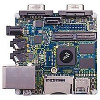
Manufacturer Part Number
MCIMX53-START
Description
KIT DEVELOPMENT I.MX53
Manufacturer
Freescale Semiconductor
Series
i.MX53r
Type
MCUr
Datasheets
1.MCIMX53-START.pdf
(2 pages)
2.MCIMX53-START.pdf
(180 pages)
3.MCIMX53-START.pdf
(204 pages)
Specifications of MCIMX53-START
Contents
Board
Silicon Manufacturer
Freescale
Core Architecture
ARM
Core Sub-architecture
Cortex - A8
Silicon Core Number
I.MX5
Silicon Family Name
I.MX53
Peak Reflow Compatible (260 C)
Yes
Rohs Compliant
Yes
Leaded Process Compatible
Yes
Lead Free Status / RoHS Status
Lead free / RoHS Compliant
For Use With/related Products
i.MX53
Lead Free Status / Rohs Status
Supplier Unconfirmed
Available stocks
Company
Part Number
Manufacturer
Quantity
Price


1
2
3
4
5
6
7
8
Electrical Characteristics
4.3.2.2
The LPDDR2 interface fully complies with JESD209-2B LPDDR2 JEDEC standard release June, 2009.
30
High-level output voltage
Low-level output voltage
Output minimum Source Current
Output min Sink Current
Input Reference Voltage
DC input High Voltage (data pins)
DC input Low Voltage (data pins)
DC Input voltage range of each
differential input
DC Differential input voltage required for
switching
Termination Voltage
Input current (no pull-up/down)
Keeper Circuit Resistance
High-level output voltage
Low-level output voltage
Input Reference Voltage
DC input High Voltage
Note that the JEDEC SSTL_18 specification (JESD8-15a) for a SSTL interface for class II operation supersedes any
specification in this document.
OVDD is the I/O power supply (1.7 V–1.9 V for DDR2)
(Vout - OVDD) / Ioh must be less than 21 Ω for values of Vout between OVDD and OVDD-0.28 V.
Vout / Iol must be less than 21 Ω for values of Vout between 0 V and 280 mV.
Vin(dc) specifies the allowable DC voltage exertion of each differential input.
Vid(dc) specifies the input differential voltage |Vtr-Vcp| required for switching, where Vtr is the “true” input level and Vcp is the
“complementary” input level. The minimum value is equal to Vih(dc) -Vil(dc).
Typ condition: 1.8 V, and 25 °C. Max condition: 1.9 V, and 105 °C.
Use an off-chip pull resistor of less than 60kΩ to override this keeper.
6
Parameters
Parameters
LPDDR2 Mode I/O DC Parameters
5
4
2
i.MX53xD Applications Processors for Consumer Products, Rev. 1
7
3
Table 12. LPDDR2 I/O DC Electrical Parameters
Table 11. DDR2 I/O DC Electrical Parameters
Voh
Vol
Ioh
Iol
Vref
Vihd
(dc)
Vild (dc)
Vin (dc)
Vid(dc)
Vtt
Iin
Voh
Vol
Vref
Vih(dc)
Symbol
Symbol
—
Test Conditions
Test Conditions
OVDD=1.7 V,
OVDD=1.7 V,
Vout=280 mV
Vout=1.42 V
VI=OVDD
VI = 0 V
Vtt
—
—
—
—
—
—
—
—
—
—
Vref+0.125V
0.49*OVDD
0.49*OVDD
Vref+0.13V
Vref – 0.04
0.9*OVDD
0.9*OVDD
–13.4
13.4
–0.3
–0.3
0.25
Min
Min
—
—
—
—
—
1
1
0.5*OVDD
0.5*OVDD
125
0.07
Vref
Typ
Typ
—
—
—
—
—
—
—
—
—
—
—
2
8
Freescale Semiconductor
Vref-0.125V
0.51*OVDD
0.51*OVDD
OVDD+0.6
Vref + 0.04
OVDD+0.3
OVDD+0.3
0.1*OVDD
0.1*OVDD
OVDD
Max
Max
360
—
—
—
—
—
5
Unit
Unit
mA
mA
kΩ
nA
V
V
V
V
V
V
V
V
V
V
Related parts for MCIMX53-START
Image
Part Number
Description
Manufacturer
Datasheet
Request
R

Part Number:
Description:
MCIMX-LVDS1
Manufacturer:
Freescale Semiconductor
Datasheet:

Part Number:
Description:
Manufacturer:
Freescale Semiconductor, Inc
Datasheet:
Part Number:
Description:
Manufacturer:
Freescale Semiconductor, Inc
Datasheet:
Part Number:
Description:
Manufacturer:
Freescale Semiconductor, Inc
Datasheet:
Part Number:
Description:
Manufacturer:
Freescale Semiconductor, Inc
Datasheet:
Part Number:
Description:
Manufacturer:
Freescale Semiconductor, Inc
Datasheet:
Part Number:
Description:
Manufacturer:
Freescale Semiconductor, Inc
Datasheet:
Part Number:
Description:
Manufacturer:
Freescale Semiconductor, Inc
Datasheet:
Part Number:
Description:
Manufacturer:
Freescale Semiconductor, Inc
Datasheet:
Part Number:
Description:
Manufacturer:
Freescale Semiconductor, Inc
Datasheet:
Part Number:
Description:
Manufacturer:
Freescale Semiconductor, Inc
Datasheet:
Part Number:
Description:
Manufacturer:
Freescale Semiconductor, Inc
Datasheet:
Part Number:
Description:
Manufacturer:
Freescale Semiconductor, Inc
Datasheet:
Part Number:
Description:
Manufacturer:
Freescale Semiconductor, Inc
Datasheet:
Part Number:
Description:
Manufacturer:
Freescale Semiconductor, Inc
Datasheet: