MCIMX53-START Freescale Semiconductor, MCIMX53-START Datasheet - Page 136
MCIMX53-START
Manufacturer Part Number
MCIMX53-START
Description
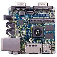
KIT DEVELOPMENT I.MX53
Manufacturer
Freescale Semiconductor
Series
i.MX53r
Type
MCUr
Datasheets
1.MCIMX53-START.pdf
(2 pages)
2.MCIMX53-START.pdf
(180 pages)
3.MCIMX53-START.pdf
(204 pages)
Specifications of MCIMX53-START
Contents
Board
Silicon Manufacturer
Freescale
Core Architecture
ARM
Core Sub-architecture
Cortex - A8
Silicon Core Number
I.MX5
Silicon Family Name
I.MX53
Peak Reflow Compatible (260 C)
Yes
Rohs Compliant
Yes
Leaded Process Compatible
Yes
Lead Free Status / RoHS Status
Lead free / RoHS Compliant
For Use With/related Products
i.MX53
Lead Free Status / Rohs Status
Supplier Unconfirmed
Available stocks
Company
Part Number
Manufacturer
Quantity
Price


Electrical Characteristics
4.7.17
4.7.17.1
The i.MX53xD UART interfaces can serve both as DTE or DCE device. This can be configured by the
DCEDTE control bit (default 0 – DCE mode).
enabled mode.
4.7.17.2
The following sections describe the electrical information of the UART module in the RS-232 mode.
4.7.17.2.1
Figure 87
Table 85
136
RXD_MUX
TXD_MUX
DCD
DTR
DSR
Port
RTS
CTS
RI
lists the UART RS-232 serial mode transmit timing characteristics.
depicts the transmit timing of UART in the RS-232 serial mode, with 8 data bit/1 stop bit format.
UART I/O Configuration and Timing Parameters
UART RS-232 I/O Configuration in Different Modes
UART RS-232 Serial Mode Timing
•
•
•
•
•
UART Transmitter
Direction
Output
Output
Output
Input
Input
Input
Input
Input
All the timings for the SSI are given for a non-inverted serial clock
polarity (TSCKP/RSCKP = 0) and a non-inverted frame sync
(TFSI/RFSI = 0). If the polarity of the clock and/or the frame sync have
been inverted, all the timing remains valid by inverting the clock signal
STCK/SRCK and/or the frame sync STFS/SRFS shown in the tables
and in the figures.
All timings are on Audiomux Pads when SSI is being used for data
transfer.
“Tx” and “Rx” refer to the Transmit and Receive sections of the SSI.
The terms WL and BL refer to Word Length (WL) and Bit Length (BL).
For internal Frame Sync operation using external clock, the FS timing is
same as that of Tx Data (for example, during AC97 mode of operation).
i.MX53xD Applications Processors for Consumer Products, Rev. 1
RTS from DTE to DCE
CTS from DCE to DTE
DTR from DTE to DCE
DSR from DCE to DTE
DCD from DCE to DTE
RING from DCE to DTE
Serial data from DCE to DTE
Serial data from DTE to DCE
Table 84. UART I/O Configuration vs. Mode
DTE Mode
Description
Table 84
NOTE
shows the UART I/O configuration based on the
Direction
Output
Output
Output
Output
Output
Input
Input
Input
RTS from DTE to DCE
CTS from DCE to DTE
DTR from DTE to DCE
DSR from DCE to DTE
DCD from DCE to DTE
RING from DCE to DTE
Serial data from DCE to DTE
Serial data from DTE to DCE
DCE Mode
Description
Freescale Semiconductor
Related parts for MCIMX53-START
Image
Part Number
Description
Manufacturer
Datasheet
Request
R

Part Number:
Description:
MCIMX-LVDS1
Manufacturer:
Freescale Semiconductor
Datasheet:

Part Number:
Description:
Manufacturer:
Freescale Semiconductor, Inc
Datasheet:
Part Number:
Description:
Manufacturer:
Freescale Semiconductor, Inc
Datasheet:
Part Number:
Description:
Manufacturer:
Freescale Semiconductor, Inc
Datasheet:
Part Number:
Description:
Manufacturer:
Freescale Semiconductor, Inc
Datasheet:
Part Number:
Description:
Manufacturer:
Freescale Semiconductor, Inc
Datasheet:
Part Number:
Description:
Manufacturer:
Freescale Semiconductor, Inc
Datasheet:
Part Number:
Description:
Manufacturer:
Freescale Semiconductor, Inc
Datasheet:
Part Number:
Description:
Manufacturer:
Freescale Semiconductor, Inc
Datasheet:
Part Number:
Description:
Manufacturer:
Freescale Semiconductor, Inc
Datasheet:
Part Number:
Description:
Manufacturer:
Freescale Semiconductor, Inc
Datasheet:
Part Number:
Description:
Manufacturer:
Freescale Semiconductor, Inc
Datasheet:
Part Number:
Description:
Manufacturer:
Freescale Semiconductor, Inc
Datasheet:
Part Number:
Description:
Manufacturer:
Freescale Semiconductor, Inc
Datasheet:
Part Number:
Description:
Manufacturer:
Freescale Semiconductor, Inc
Datasheet: