TRC105 RFM, TRC105 Datasheet - Page 7
TRC105
Manufacturer Part Number
TRC105
Description
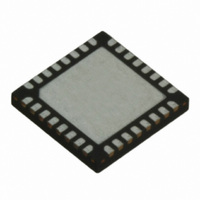
IC TXRX 300MHZ-510MHZ 32TQFN
Manufacturer
RFM
Specifications of TRC105
Frequency
300MHz ~ 510MHz
Data Rate - Maximum
200kbps
Modulation Or Protocol
FSK, OOK
Applications
General Purpose
Power - Output
13dBm
Sensitivity
-112dBm
Voltage - Supply
2.1 V ~ 3.6 V
Current - Receiving
3mA
Current - Transmitting
30mA
Data Interface
PCB, Surface Mount
Antenna Connector
PCB, Surface Mount
Operating Temperature
-40°C ~ 85°C
Package / Case
32-TQFN
Wireless Frequency
300 MHz to 510 MHz
Output Power
13 dBm
Operating Supply Voltage
2.1 V to 3.6 V
Maximum Operating Temperature
+ 85 C
Mounting Style
SMD/SMT
Maximum Supply Current
1.7 mA
Minimum Operating Temperature
- 40 C
Modulation
FSK, OOK
Lead Free Status / RoHS Status
Lead free / RoHS Compliant
Memory Size
-
Lead Free Status / Rohs Status
Lead free / RoHS Compliant
Other names
583-1159-2


2.1 RF Port
The receiver and the transmitter share the same RF pins. Figure 3 shows the implementation of the common
front-end. In transmit mode, the PA and the PA regulator are on; the voltage on VDD_PA pin is the nominal volt-
age of the regulator, about 1.8 V. The external inductances L1 and L4 are used for the PA. In receive mode, both
PA and PA regulator are off, and VDD_PA is tied to ground. The external inductances L1 and L4 are used for bi-
asing and matching the LNA, which is implemented as a common gate amplifier.
2.2 Transmitter
The TRC105 is set to transmit mode when MCFG00_Chip_Mode[7..5] bits are set to 100. In Continuous data
mode the transmitted data is sent directly to the modulator. The host microcontroller is provided with a bit rate
clock by the TRC105 to clock the data; using this clock to send the data synchronously is mandatory in FSK con-
figuration and optional in OOK configuration. In Buffered and Packet data modes the data is first written into the
64-byte FIFO via the SPI interface; data from the FIFO is then used by the modulator.
At the front end of the transmitter, I and Q signals are generated by the base-band circuit which contains a digital
waveform generator, two D/A converters and two anti-aliasing low-pass filters. The I and Q signals are two quad-
rature sinusoids whose frequency is the selected frequency deviation. In FSK mode, the phase shift between I
and Q is switched between +90° and -90° according to the input data. The modulation is then performed at this
stage, since the information contained in the phase shift will be converted into a frequency shift when the I and Q
signals are combined in the first mixers. In OOK mode, the phase shift is kept constant whatever the data. The
combination of the I and Q signals in the first mixers creates a fixed frequency signal at a low intermediate fre-
quency which is equal to the selected frequency deviation. After D/A conversion, both I and Q signals are filtered
by anti-aliasing filters whose bandwidth is programmed with the register TXCFG1A_TXInterpfilt[7..4]. Behind the
filters, a set of four mixers combines the I and Q signals and converts them into two I and Q signals at the second
intermediate frequency which is equal to 1/8 of the LO frequency, which in turn is equal to 8/9 of the RF fre-
quency. These two new I and Q signals are then combined and up-converted to the desired RF frequency by two
quadrature mixers fed by the LO signals. The signal is then amplified by a driver and power amplifier stage.
www.RFM.com
©2009-2010 by RF Monolithics, Inc.
E-mail:
info@rfm.com
MCFG05_PA_Ramp[7..6]
00
01
10
11
Technical support +1.800.704.6079
Figure 3
Table 2
T
PA
8.5
15
23
3
(µs)
Rise/fall (µs)
20/10
2.5/2
10/6
5/3
TRC105 - 11/01/10
Page 7 of 66
Related parts for TRC105
Image
Part Number
Description
Manufacturer
Datasheet
Request
R

Part Number:
Description:
TRANSCEIVER RF 916MHZ 1/2-DUPLEX
Manufacturer:
Linx Technologies Inc
Datasheet:
Part Number:
Description:
TRANSCEIVER RF 916MHZ 1/2-DUPLEX
Manufacturer:
Linx Technologies Inc
Datasheet:
Part Number:
Description:
TXCVR RF 900MHZ 1/2-DUPLEX 180CH
Manufacturer:
Linx Technologies Inc
Part Number:
Description:
TRANSCEIVER RF 916MHZ 20PIN SMD
Manufacturer:
Linx Technologies Inc
Datasheet:

Part Number:
Description:
ASH TR 115.2 KBPS 433.92 MHZ
Manufacturer:
RFM
Datasheet:

Part Number:
Description:
ASH TR 115.2 KBPS 916.5 MHZ
Manufacturer:
RFM
Datasheet:

Part Number:
Description:
ASH TR 115.2 KBPS 433.92 MHZ
Manufacturer:
RFM
Datasheet:
Part Number:
Description:
ASH TR 115.2 KBPS 916.5 MHZ
Manufacturer:
RFM
Datasheet:

Part Number:
Description:
ASH TR 115.2 KBPS 403.5 MHZ
Manufacturer:
RFM
Datasheet:

Part Number:
Description:
ASH RX 115.2 KBPS 433.92 MHZ
Manufacturer:
RFM
Datasheet:

Part Number:
Description:
10-Terminal Ceramic Surface-Mount Case 7 x 5 mm Nominal Footprint
Manufacturer:
RFM [RF Monolithics, Inc]
Datasheet:
Part Number:
Description:
QUAD-BAND GSM850/GSM/DCS/PCS POWER AMP MODULE
Manufacturer:
RFM [RF Monolithics, Inc]
Datasheet:
Part Number:
Description:
402 to 405 MHz Medical Band Front-end Filter
Manufacturer:
RFM [RF Monolithics, Inc]
Datasheet:
Part Number:
Description:
674.03 MHz SAW Resonator
Manufacturer:
RFM [RF Monolithics, Inc]
Datasheet: