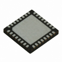
TRC105 RFM, TRC105 Datasheet - Page 14

TRC105
Manufacturer Part Number
TRC105
Description
IC TXRX 300MHZ-510MHZ 32TQFN
Manufacturer
RFM
Specifications of TRC105
Frequency
300MHz ~ 510MHz
Data Rate - Maximum
200kbps
Modulation Or Protocol
FSK, OOK
Applications
General Purpose
Power - Output
13dBm
Sensitivity
-112dBm
Voltage - Supply
2.1 V ~ 3.6 V
Current - Receiving
3mA
Current - Transmitting
30mA
Data Interface
PCB, Surface Mount
Antenna Connector
PCB, Surface Mount
Operating Temperature
-40°C ~ 85°C
Package / Case
32-TQFN
Wireless Frequency
300 MHz to 510 MHz
Output Power
13 dBm
Operating Supply Voltage
2.1 V to 3.6 V
Maximum Operating Temperature
+ 85 C
Mounting Style
SMD/SMT
Maximum Supply Current
1.7 mA
Minimum Operating Temperature
- 40 C
Modulation
FSK, OOK
Lead Free Status / RoHS Status
Lead free / RoHS Compliant
Memory Size
-
Lead Free Status / Rohs Status
Lead free / RoHS Compliant
Other names
583-1159-2
3.2 Continuous Mode Data and Clock Recovery
The raw output signal from the demodulator may contain jitter and glitches. Data and clock recovery converts the
data output of the demodulator into a glitch-free bit-stream DATA and generates a synchronized clock DCLK to be
used for sampling the DATA output as shown in Figure 8. DCLK is available on pin IRQ1 when the TRC105 oper-
ates in continuous mode.
To ensure correct operation of the data and clock recovery circuit, the following conditions have to be satisfied:
Data and clock recovery is enabled by default. It is controlled by RXCFG12_DCLK_Dis[6]. If data and clock re-
covery is disabled, the output of the demodulator is directed to DATA and the DCLK output (IRQ1 Pin in continu-
ous mode) is set to 0.
The received bit rate is defined by the values of the MCFG03 and MCFG04 configuration registers, and is calcu-
lated as follows:
with BR the bit rate in kb/s, F
MCFG04. For example, using a 12.8 MHz crystal (12,800 kHz), the bit rate is 25 kb/s when C = 7 and D = 31.
3.3 Continuous Mode Start Pattern Detection
Start pattern detection is activated by setting the RXCFG12_Recog[5] bit to 1. The demodulated signal is com-
pared with a pattern stored in the SYNCFG registers. The Start Pattern Detect signal (PATTERN), is driven by the
output of this comparator and is synchronized by DCLK. It is set to 1 when a pattern match is detected, otherwise
set to 0. The pattern detect output is updated at the rising edge of DCLK. The number of bytes used for compari-
son is defined in the RXCFG12_Pat_sz[4..3] register and the number of tolerated bit errors for pattern detection
is defined in the RXCFG12_Ptol[2..1] register. Figure 9 illustrates the pattern detection process.
www.RFM.com
©2009-2010 by RF Monolithics, Inc.
•
•
•
BR = F
A 1-0-1-0… preamble of at least 24 bits is required for synchronization
The transmitted bit stream must have at least one transition from 0 to 1 or from 1 to 0 every 8 bits during
transmission
The bit rate accuracy must be better than 2 %.
E-mail:
XTAL
/(2*(C + 1)*(D + 1)), with C in the range of 0 to 255, and D = 31 (suitable for most applications)
info@rfm.com
XTAL
the crystal frequency in kHz, C the value in MCFG03, and D the value in
Technical support +1.800.704.6079
Figure 8
TRC105 - 11/01/10
Page 14 of 66


