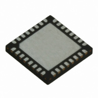
TRC105 RFM, TRC105 Datasheet - Page 15

TRC105
Manufacturer Part Number
TRC105
Description
IC TXRX 300MHZ-510MHZ 32TQFN
Manufacturer
RFM
Specifications of TRC105
Frequency
300MHz ~ 510MHz
Data Rate - Maximum
200kbps
Modulation Or Protocol
FSK, OOK
Applications
General Purpose
Power - Output
13dBm
Sensitivity
-112dBm
Voltage - Supply
2.1 V ~ 3.6 V
Current - Receiving
3mA
Current - Transmitting
30mA
Data Interface
PCB, Surface Mount
Antenna Connector
PCB, Surface Mount
Operating Temperature
-40°C ~ 85°C
Package / Case
32-TQFN
Wireless Frequency
300 MHz to 510 MHz
Output Power
13 dBm
Operating Supply Voltage
2.1 V to 3.6 V
Maximum Operating Temperature
+ 85 C
Mounting Style
SMD/SMT
Maximum Supply Current
1.7 mA
Minimum Operating Temperature
- 40 C
Modulation
FSK, OOK
Lead Free Status / RoHS Status
Lead free / RoHS Compliant
Memory Size
-
Lead Free Status / Rohs Status
Lead free / RoHS Compliant
Other names
583-1159-2
Figure 9
Note that start pattern detection is enabled only if data and clock recovery is enabled.
3.4 RSSI
The received signal strength is measured in the amplifier chains behind the second mixers. Each amplifier chain
is composed of 11 amplifiers each having a gain of 6 dB and an intermediate output at 3 dB. By monitoring the
two outputs of each stage, an estimation of the signal strength with a resolution of 3 dB and a dynamic range of
63 dB is obtained. This estimation is performed 16 times over a period of the I and Q signals and the 16 samples
are averaged to obtain a final RSSI value with a 0.5 dB step. The period of the I and Q signal is the inverse of the
deviation frequency, which is the low-IF frequency in OOK mode. The RSSI effective dynamic range can be in-
creased to 70 dB by adjusting MCFG01_IF_Gain[1..0] for less gain on high signal levels.
The RSSI block can also be used in interrupt mode by setting the bit IRQCFG0E_RSSI_Int[3] to 1. When
RXCFG14_RSSI is equal or greater than a predefined value stored in IRQCFG0F_RSSI_thld, bit IRQCFG0E_
SIG_DETECT[2] goes high and an interrupt signal RSSI_IRQ is generated on pin IRQ0 if IRQCFG0D_RX_
IRQ0[7..6] is set to 01 (see Table 10). The interrupt is cleared by writing a 1 to bit IRQCFG0E_ SIG_DETECT[2].
If the bit RSSI_IRQ remains high, the process starts again. Figure 10 shows the timing diagram of RSSI in inter-
rupt mode.
Figure 10
3.5 Receiving in Buffered Data Mode
The receiver works in Buffered data mode when the MCFG01_Mode[7..6] bits are set to 01. In this mode, the
output of the data and clock recovery, i.e., the demodulated and resynchronized signal and the clock signal DCLK
are not sent directly to the output pins DATA and IRQ1 (DCLK). These signals are used to store the demodulated
data in blocks of 8 bits in a 64-byte FIFO. Figure 11 shows the receiver chain in this mode. The FSK and OOK
demodulators, data and clock recovery circuit and start pattern detect block work as described for Continuous
data mode, but they are used with two additional blocks, the FIFO and SPI.
www.RFM.com
E-mail:
info@rfm.com
Technical support +1.800.704.6079
Page 15 of 66
©2009-2010 by RF Monolithics, Inc.
TRC105 - 11/01/10


