TRC105 RFM, TRC105 Datasheet - Page 17
TRC105
Manufacturer Part Number
TRC105
Description
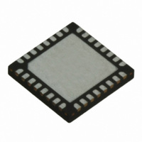
IC TXRX 300MHZ-510MHZ 32TQFN
Manufacturer
RFM
Specifications of TRC105
Frequency
300MHz ~ 510MHz
Data Rate - Maximum
200kbps
Modulation Or Protocol
FSK, OOK
Applications
General Purpose
Power - Output
13dBm
Sensitivity
-112dBm
Voltage - Supply
2.1 V ~ 3.6 V
Current - Receiving
3mA
Current - Transmitting
30mA
Data Interface
PCB, Surface Mount
Antenna Connector
PCB, Surface Mount
Operating Temperature
-40°C ~ 85°C
Package / Case
32-TQFN
Wireless Frequency
300 MHz to 510 MHz
Output Power
13 dBm
Operating Supply Voltage
2.1 V to 3.6 V
Maximum Operating Temperature
+ 85 C
Mounting Style
SMD/SMT
Maximum Supply Current
1.7 mA
Minimum Operating Temperature
- 40 C
Modulation
FSK, OOK
Lead Free Status / RoHS Status
Lead free / RoHS Compliant
Memory Size
-
Lead Free Status / Rohs Status
Lead free / RoHS Compliant
Other names
583-1159-2


th
nFIFOEMPY[0] is reset. When the last bit of the 64
byte has been written into the FIFO, signal IRQCFG0D_
FIFOFULL[1] is set. Data must be read before the next byte is received or it will be overwritten.
The IRQCFG0D_nFIFOEMPY[0] signal can be used as an interrupt signal for the host microcontroller by map-
ping to pin IRQ0 if IRQCFG0D_RX_IRQ0[7..6] is set to 10. Alternatively, the WRITE_byte signal may also be
used as an interrupt if IRQCFG0D_RX_IRQ0[7..6] is set to 01.
Demodulation in buffered mode occurs in the same way as in continuous mode. Received data is directly read
from the FIFO and the DATA and DCLK pins are not used. Data and clock recovery in buffered mode is automati-
cally enabled. DCLK is not externally available.
The pattern recognition block is automatically enabled in Buffered data mode. The Start Pattern Detect
(PATTERN) signal can be mapped to pin IRQ0. In Buffered data mode RSSI operates the same way as in Con-
tinuous data mode. However, RSSI_IRQ may be mapped to IRQ1 instead of to IRQ0 in Continuous data mode.
Figure 12
3.6 Transmitting in Continuous or Buffered Data Modes
The transmitter operates in Continuous data mode when the MCFG01_Mode [7..6] bits are set to 00. Bit clock
DCLK is available on pin IRQ1. Bits are clocked into the transmitter on the rising edge of this clock. Data must be
stable 2 µs before the rising edge of DCLK and must be held for 2 µs following the rising edge of this clock
(T
). To meet this requirement, data can be changed on the falling edge of DCLK. In FSK mode DCLK must
SUDATA
be used but is optional in OOK mode.
The transmitter operates in Buffered data mode when the MCFG01_Mode [5] bit is set to 1. Data to be transmit-
ted is written to the 64-byte FIFO through the SPI interface. FIFO data is loaded byte-by-byte into a shift register
which then transfers the data bit-by-bit to the modulator. FIFO operation in transmit mode is similar to receive
mode. Transmission can start immediately after the first byte of data is written into the FIFO or when the FIFO is
full, as determined by the IRQCFG0E_Start_Full[4] bit setting. If the transmit FIFO is full, the interrupt signal
IRQCFG0D_ FIFOFULL[2] is asserted on pin IRQ1. If data is written into the FIFO while it is full, the flag
IRQCFG0D_FIFO_OVR[0] will be set to 1 and the previous FIFO contents will be overwritten. The IRQCFG0D_
FIFO_OVR[0] flag is cleared by writing a 1 to it. At the same time the contents of the FIFO are cleared. Once the
last data byte in the FIFO is loaded into the shift register driving the transmitter modulator, the flag IRQCFG0D_
nFIFOEMPY[1] is set to 0 on pin IRQ0. If new data is not written to the FIFO and the last bit has been transferred
to the modulator, the IRQCFG0E_TX_ STOP[5] bit goes high as the modulator starts to send the last bit. The
transmitter must remain on one bit period after TX_STOP to transmit the last bit. If the transmitter is switched off
(switched to another mode), the transmission stops immediately even if there is still data in the shift register. In
www.RFM.com
E-mail:
info@rfm.com
Technical support +1.800.704.6079
Page 17 of 66
©2009-2010 by RF Monolithics, Inc.
TRC105 - 11/01/10
Related parts for TRC105
Image
Part Number
Description
Manufacturer
Datasheet
Request
R

Part Number:
Description:
TRANSCEIVER RF 916MHZ 1/2-DUPLEX
Manufacturer:
Linx Technologies Inc
Datasheet:
Part Number:
Description:
TRANSCEIVER RF 916MHZ 1/2-DUPLEX
Manufacturer:
Linx Technologies Inc
Datasheet:
Part Number:
Description:
TXCVR RF 900MHZ 1/2-DUPLEX 180CH
Manufacturer:
Linx Technologies Inc
Part Number:
Description:
TRANSCEIVER RF 916MHZ 20PIN SMD
Manufacturer:
Linx Technologies Inc
Datasheet:

Part Number:
Description:
ASH TR 115.2 KBPS 433.92 MHZ
Manufacturer:
RFM
Datasheet:

Part Number:
Description:
ASH TR 115.2 KBPS 916.5 MHZ
Manufacturer:
RFM
Datasheet:

Part Number:
Description:
ASH TR 115.2 KBPS 433.92 MHZ
Manufacturer:
RFM
Datasheet:
Part Number:
Description:
ASH TR 115.2 KBPS 916.5 MHZ
Manufacturer:
RFM
Datasheet:

Part Number:
Description:
ASH TR 115.2 KBPS 403.5 MHZ
Manufacturer:
RFM
Datasheet:

Part Number:
Description:
ASH RX 115.2 KBPS 433.92 MHZ
Manufacturer:
RFM
Datasheet:

Part Number:
Description:
10-Terminal Ceramic Surface-Mount Case 7 x 5 mm Nominal Footprint
Manufacturer:
RFM [RF Monolithics, Inc]
Datasheet:
Part Number:
Description:
QUAD-BAND GSM850/GSM/DCS/PCS POWER AMP MODULE
Manufacturer:
RFM [RF Monolithics, Inc]
Datasheet:
Part Number:
Description:
402 to 405 MHz Medical Band Front-end Filter
Manufacturer:
RFM [RF Monolithics, Inc]
Datasheet:
Part Number:
Description:
674.03 MHz SAW Resonator
Manufacturer:
RFM [RF Monolithics, Inc]
Datasheet: