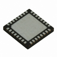
TRC105 RFM, TRC105 Datasheet - Page 60

TRC105
Manufacturer Part Number
TRC105
Description
IC TXRX 300MHZ-510MHZ 32TQFN
Manufacturer
RFM
Specifications of TRC105
Frequency
300MHz ~ 510MHz
Data Rate - Maximum
200kbps
Modulation Or Protocol
FSK, OOK
Applications
General Purpose
Power - Output
13dBm
Sensitivity
-112dBm
Voltage - Supply
2.1 V ~ 3.6 V
Current - Receiving
3mA
Current - Transmitting
30mA
Data Interface
PCB, Surface Mount
Antenna Connector
PCB, Surface Mount
Operating Temperature
-40°C ~ 85°C
Package / Case
32-TQFN
Wireless Frequency
300 MHz to 510 MHz
Output Power
13 dBm
Operating Supply Voltage
2.1 V to 3.6 V
Maximum Operating Temperature
+ 85 C
Mounting Style
SMD/SMT
Maximum Supply Current
1.7 mA
Minimum Operating Temperature
- 40 C
Modulation
FSK, OOK
Lead Free Status / RoHS Status
Lead free / RoHS Compliant
Memory Size
-
Lead Free Status / Rohs Status
Lead free / RoHS Compliant
Other names
583-1159-2
The SPI interface is used with Packet data mode as with Buffered data mode. IRQ0 and IRQ1 mapping is config-
ured in register IRQCFG0D. Bits 7..6 select the signal for IRQ0 in the receive mode. In transmit mode, IRQ0
mapping is set by IRQCFG0D bit 3. IRQCFG0D bits 5..4 select the signal for IRQ1 in the receive mode. Bit 3 se-
lects the IRQ1 signal in transmit mode. The mapping options for Packet data mode are summarized in Table 81
below:
In addition, IRQCFG0E allows several internal interrupts to be configured. See Table 82 below:
www.RFM.com
©2009-2010 by RF Monolithics, Inc.
•
•
•
•
•
Recognition of start pattern in receive mode
Automatic removal of preamble and start pattern in receive mode (payload only in FIFO)
Flagging of received packets with errors or flagging and discard of packets with errors
Filtering of received packets based on address byte - address match only, address byte plus 0x00 broad-
cast address or address byte plus 0x00 and 0xFF broadcast addresses
New IRQ0 and IRQ1 mapping options
E-mail:
IRQCFG0D bits
IRQCFG0E bits
7..6
7..6
7..6
7..6
5..4
5..4
5..4
5..4
3
3
3
3
7
7
6
6
5
5
4
4
3
3
2
2
1
1
0
0
info@rfm.com
Cfg
Cfg
00
01
10
11
00
01
10
11
1
0
0
1
0
1
0
1
0
1
0
1
0
1
1
0
1
0
1
0
State
RX
RX
RX
RX
RX
RX
RX
RX
TX
TX
TX
TX
Technical support +1.800.704.6079
IRQ
PLL_LOCK signal disabled (bit 1 above), Pin 23 set high
Stop filling FIFO (if bit 7 is 0, this is Start Pattern Detect)
0
0
0
0
0
1
1
1
1
0
1
1
Start FIFO fill when start pattern detected
Write_byte (high pulse when received byte written to FIFO)
Table 81
Table 82
FIFO overflow (write 1 to reset FIFO)
Transmitting all pending bits in FIFO
Disable RSSI interrupt (bit 2)
Enable RSSI interrupt (bit 2)
RF signal < RSSI Threshold
RF signal ≥ RSSI threshold
Internal Interrupt Control
All bits in FIFO transmitted
PLL_LOCK signal enabled
Start Pattern Detect or Node Address Match
Control FIFO with bit 6
nFIFOEMPY (low when FIFO is empty)
Start filling FIFO
PLL not locked
PLL locked
FIFO OK
Data_Rdy (CRC OK)
FIFO_Int_Rx
FIFO_Int_Tx
nFIFOEMPY
FIFOFULL
FIFOFULL
RSSI_IRQ
CRC_OK
TX_Stop
Source
TRC105 - 11/01/10
Page 60 of 66


