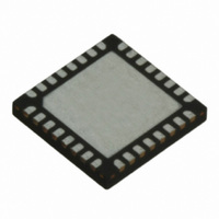
TRC105 RFM, TRC105 Datasheet - Page 27

TRC105
Manufacturer Part Number
TRC105
Description
IC TXRX 300MHZ-510MHZ 32TQFN
Manufacturer
RFM
Specifications of TRC105
Frequency
300MHz ~ 510MHz
Data Rate - Maximum
200kbps
Modulation Or Protocol
FSK, OOK
Applications
General Purpose
Power - Output
13dBm
Sensitivity
-112dBm
Voltage - Supply
2.1 V ~ 3.6 V
Current - Receiving
3mA
Current - Transmitting
30mA
Data Interface
PCB, Surface Mount
Antenna Connector
PCB, Surface Mount
Operating Temperature
-40°C ~ 85°C
Package / Case
32-TQFN
Wireless Frequency
300 MHz to 510 MHz
Output Power
13 dBm
Operating Supply Voltage
2.1 V to 3.6 V
Maximum Operating Temperature
+ 85 C
Mounting Style
SMD/SMT
Maximum Supply Current
1.7 mA
Minimum Operating Temperature
- 40 C
Modulation
FSK, OOK
Lead Free Status / RoHS Status
Lead free / RoHS Compliant
Memory Size
-
Lead Free Status / Rohs Status
Lead free / RoHS Compliant
Other names
583-1159-2
Figure 20 shows the timing diagram for a single byte write sequence to the TRC105 through the SPI configuration
interface. Note that nSS_CONFIG must remain low during the transmission of the two bytes (address and data). If
it goes high after the first byte, then the next byte will be considered as an address byte. When writing more than
one register successively, nSS_CONFIG does not need to have a high-to-low transition between two write se-
quences. The bytes are alternatively considered as an address byte followed by a data byte.
The read sequence through the SPI configuration interface is similar to the write sequence. The host microcon-
troller sends the address during the first SPI communication and then reads the data during a second SPI com-
munication. Note that 0 bits can be input to the SDI during the second SPI communication for a single byte read.
Figure 21 shows the timing diagram for a single byte read sequence from the TRC105 through the SPI.
Multiple configuration register reads are also possible by sending a series of register addresses into the SPI port,
as shown in Figure 22.
3.11 SPI Data FIFO Interface
When the transceiver is used in Buffered or Packet data mode, data is written to and read from the FIFO through
the SPI interface. Two interrupts, IRQ0 and IRQ1, are used to manage the transfer procedure.
When the transceiver is operating in Buffered or Packet data mode, the FIFO interface is selected when
nSS_DATA is set to 0 and nSS_CONFIG is set to 1. SPI operations with the FIFO are similar to operations with
the configuration registers with two important exceptions. First, no addresses are used with the FIFO, only data
bytes are exchanged. Second, nSS_DATA must be toggled high and back low between data bytes when writing
to the FIFO or reading from the FIFO. Toggling nSS_DATA indexes the access pointer to each byte in the FIFO in
lieu of using explicit addressing. Figure 23 shows the timing diagram for a multiple-byte write sequence to the
TRC105 during transmit, and Figure 24 shows the timing for a multi-byte read sequence.
www.RFM.com
©2009-2010 by RF Monolithics, Inc.
E-mail:
info@rfm.com
Technical support +1.800.704.6079
Figure 21
Figure 22
TRC105 - 11/01/10
Page 27 of 66


