TRC105 RFM, TRC105 Datasheet - Page 55
TRC105
Manufacturer Part Number
TRC105
Description
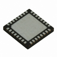
IC TXRX 300MHZ-510MHZ 32TQFN
Manufacturer
RFM
Specifications of TRC105
Frequency
300MHz ~ 510MHz
Data Rate - Maximum
200kbps
Modulation Or Protocol
FSK, OOK
Applications
General Purpose
Power - Output
13dBm
Sensitivity
-112dBm
Voltage - Supply
2.1 V ~ 3.6 V
Current - Receiving
3mA
Current - Transmitting
30mA
Data Interface
PCB, Surface Mount
Antenna Connector
PCB, Surface Mount
Operating Temperature
-40°C ~ 85°C
Package / Case
32-TQFN
Wireless Frequency
300 MHz to 510 MHz
Output Power
13 dBm
Operating Supply Voltage
2.1 V to 3.6 V
Maximum Operating Temperature
+ 85 C
Mounting Style
SMD/SMT
Maximum Supply Current
1.7 mA
Minimum Operating Temperature
- 40 C
Modulation
FSK, OOK
Lead Free Status / RoHS Status
Lead free / RoHS Compliant
Memory Size
-
Lead Free Status / Rohs Status
Lead free / RoHS Compliant
Other names
583-1159-2


The RF channel frequency for OOK transmit is:
Where F
less than (P+1), and R has a value in the range of 64 to 169. An F
ues of P, S and R for OOK transmit operation on several common frequencies are given in Table 74 for a
0.1 MHz F
6.6 TRC105 Data Mode Selection and Configuration
The TRC105 supports three data modes: Continuous, Buffered and Packet. Continuous data mode provides the
most formatting flexibility, but places the heaviest demand on host microcontroller resources and requires the
most custom firmware development. In contrast, the Packet data mode unloads the host processor and the appli-
cation firmware from handing tasks such as DC-balanced data encoding, packet frame assembly and disassem-
bly, error detection, packet filtering and FIFO buffering. The trade-off for Packet data mode is limited flexibility in
data formatting parameters such as packet frame design. Buffered data mode falls between packet and Continu-
ous data mode capabilities, providing FIFO buffering, but allowing considerable flexibility in the design of the
packet frame.
Packet data mode is generally preferred as it supports the fastest application development time and requires the
smallest and least expensive host microcontroller. Buffered data mode covers applications that require a specific
packet frame design to support features such as multi-hop routing. Continuous data mode is reserved for special-
ized requirements, such as compatibility with a legacy product.
MCFG01 bits 7..6 select the data mode. An 00 bit pattern selects Continuous data mode. A 01 bit pattern selects
Buffered data mode. Bit patterns 10 or 11 select Packet data mode. The TRC105 configuration details for each
data mode are discussed below.
6.6.1 Continuous Data Mode
In Continuous data mode operation, transmitted data streams are applied to DATA Pin 20, and received data
streams are output on Pin 20. IRQ1 Pin 22 is usually configured to supply a clock signal to the host micro-
controller to pace the transmitted and received data steams. The clock signal is generated at the configured bit
rate. When transmitting, bits are clocked into Pin 20 on the low-to-high clock transitions at Pin 22.
www.RFM.com
©2009-2010 by RF Monolithics, Inc.
F
RXRF
RXRF
IF2
. Software for determining P, S and R values is provided with the TRC105 development kit.
and the OOK 2
E-mail:
= (14.4*(75*(P + 1) + S)/(R + 1)) - F
info@rfm.com
nd
IF frequency F
MCFG00 bits 4..2
MCFG00 bits 4..2
Configuration
Configuration
R
R
P
S
P
S
Technical support +1.800.704.6079
IF2
are in MHz, and P, S, and R are divider integers where S must be
IF2
315 MHz
315 MHz
, with P, S in the range 0 to 255, R in the range of 64 to 169
Table 73
Table 74
000
143
000
143
41
41
1
1
434 MHz
434 MHz
011
191
011
191
76
13
76
13
IF2
value of 0.1 MHz is normally used. The val-
447 MHz
447 MHz
100
143
100
143
58
46
58
46
TRC105 - 11/01/10
Page 55 of 66
Related parts for TRC105
Image
Part Number
Description
Manufacturer
Datasheet
Request
R

Part Number:
Description:
TRANSCEIVER RF 916MHZ 1/2-DUPLEX
Manufacturer:
Linx Technologies Inc
Datasheet:
Part Number:
Description:
TRANSCEIVER RF 916MHZ 1/2-DUPLEX
Manufacturer:
Linx Technologies Inc
Datasheet:
Part Number:
Description:
TXCVR RF 900MHZ 1/2-DUPLEX 180CH
Manufacturer:
Linx Technologies Inc
Part Number:
Description:
TRANSCEIVER RF 916MHZ 20PIN SMD
Manufacturer:
Linx Technologies Inc
Datasheet:

Part Number:
Description:
ASH TR 115.2 KBPS 433.92 MHZ
Manufacturer:
RFM
Datasheet:

Part Number:
Description:
ASH TR 115.2 KBPS 916.5 MHZ
Manufacturer:
RFM
Datasheet:

Part Number:
Description:
ASH TR 115.2 KBPS 433.92 MHZ
Manufacturer:
RFM
Datasheet:
Part Number:
Description:
ASH TR 115.2 KBPS 916.5 MHZ
Manufacturer:
RFM
Datasheet:

Part Number:
Description:
ASH TR 115.2 KBPS 403.5 MHZ
Manufacturer:
RFM
Datasheet:

Part Number:
Description:
ASH RX 115.2 KBPS 433.92 MHZ
Manufacturer:
RFM
Datasheet:

Part Number:
Description:
10-Terminal Ceramic Surface-Mount Case 7 x 5 mm Nominal Footprint
Manufacturer:
RFM [RF Monolithics, Inc]
Datasheet:
Part Number:
Description:
QUAD-BAND GSM850/GSM/DCS/PCS POWER AMP MODULE
Manufacturer:
RFM [RF Monolithics, Inc]
Datasheet:
Part Number:
Description:
402 to 405 MHz Medical Band Front-end Filter
Manufacturer:
RFM [RF Monolithics, Inc]
Datasheet:
Part Number:
Description:
674.03 MHz SAW Resonator
Manufacturer:
RFM [RF Monolithics, Inc]
Datasheet: