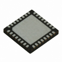
TRC105 RFM, TRC105 Datasheet - Page 11

TRC105
Manufacturer Part Number
TRC105
Description
IC TXRX 300MHZ-510MHZ 32TQFN
Manufacturer
RFM
Specifications of TRC105
Frequency
300MHz ~ 510MHz
Data Rate - Maximum
200kbps
Modulation Or Protocol
FSK, OOK
Applications
General Purpose
Power - Output
13dBm
Sensitivity
-112dBm
Voltage - Supply
2.1 V ~ 3.6 V
Current - Receiving
3mA
Current - Transmitting
30mA
Data Interface
PCB, Surface Mount
Antenna Connector
PCB, Surface Mount
Operating Temperature
-40°C ~ 85°C
Package / Case
32-TQFN
Wireless Frequency
300 MHz to 510 MHz
Output Power
13 dBm
Operating Supply Voltage
2.1 V to 3.6 V
Maximum Operating Temperature
+ 85 C
Mounting Style
SMD/SMT
Maximum Supply Current
1.7 mA
Minimum Operating Temperature
- 40 C
Modulation
FSK, OOK
Lead Free Status / RoHS Status
Lead free / RoHS Compliant
Memory Size
-
Lead Free Status / Rohs Status
Lead free / RoHS Compliant
Other names
583-1159-2
2.6 PLL Loop Filter
The loop filter for the frequency synthesizer is shown in Figure 6.
Recommended component values for the frequency synthesizer loop filter are provided in Table 6. The loop filter
settings are not dependent on the frequency band, so they can used on all designs. PLL lock status can be pro-
vided on Pin 23 by setting the IRQCFG0E_PLL_LOCK_EN[0] bit to a 1. Pin 23 goes high when the PLL is
locked. The lock status of the PLL can also be checked by reading the IRQCFG0E_PLL_ LOCK_ST[1] bit. This
bit latches high each time the PLL locks and must be reset by writing a 1 to it.
3.0 Operating Modes
The TRC105 has 5 possible chip-level modes. The chip-level mode is set by MCFG00_Chip_Mode[7..5], which
is a 3-bit pattern in the configuration register. Table 7 summarizes the chip-level modes:
Table 8 gives the state of the digital pins for the different chip-level modes and settings:
www.RFM.com
©2009-2010 by RF Monolithics, Inc.
E-mail:
MCFG00_Chip_Mode[7..5]
info@rfm.com
PLL Loop Filter
Figure 6
PIN Function
nSS_CONFIG*
nSS_DATA*
IRQ0
IRQ1
DATA
CLKOUT
SDO**
SDI
SCK
0 0 0
0 0 1
0 1 0
0 1 1
1 0 0
I = Input, O = Output, TRI = High Impedance
*nSS_CONFIG has priority OVER nSS_DATA
**SDO is an output if nSS_CONFIG = 0 and/or nSS_DATA = 0
Sleep
Mode
TRI/O
TRI
TRI
TRI
TRI
I
I
I
I
Technical support +1.800.704.6079
Chip-level Mode
Synthesizer
Transmit
Standby
Receive
Sleep
Standby
TRI/O
Mode
TRI
O
O
O
I
I
I
I
Table 7
Table 8
Synthesizer
Enabled Functions
None
Crystal oscillator
Crystal and frequency synthesizer
Crystal, frequency synthesizer and receiver
Crystal, frequency synthesizer and transmitter
Mode
TRI/O
PLL Loop Filter Components
TRI
O
O
O
I
I
I
I
Name
C8
C9
R1
Receive
Mode
TRI/O
O
O
O
O
1000 pF
6800 pF
I
I
I
I
6.8 kΩ
Value
Table 6
Transmit
TRI/O
Mode
Tolerance
O
O
O
I
I
I
I
I
±10%
±10%
±5%
TRC105 - 11/01/10
Page 11 of 66


