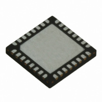
TRC105 RFM, TRC105 Datasheet - Page 62

TRC105
Manufacturer Part Number
TRC105
Description
IC TXRX 300MHZ-510MHZ 32TQFN
Manufacturer
RFM
Specifications of TRC105
Frequency
300MHz ~ 510MHz
Data Rate - Maximum
200kbps
Modulation Or Protocol
FSK, OOK
Applications
General Purpose
Power - Output
13dBm
Sensitivity
-112dBm
Voltage - Supply
2.1 V ~ 3.6 V
Current - Receiving
3mA
Current - Transmitting
30mA
Data Interface
PCB, Surface Mount
Antenna Connector
PCB, Surface Mount
Operating Temperature
-40°C ~ 85°C
Package / Case
32-TQFN
Wireless Frequency
300 MHz to 510 MHz
Output Power
13 dBm
Operating Supply Voltage
2.1 V to 3.6 V
Maximum Operating Temperature
+ 85 C
Mounting Style
SMD/SMT
Maximum Supply Current
1.7 mA
Minimum Operating Temperature
- 40 C
Modulation
FSK, OOK
Lead Free Status / RoHS Status
Lead free / RoHS Compliant
Memory Size
-
Lead Free Status / Rohs Status
Lead free / RoHS Compliant
Other names
583-1159-2
PKTCFG1E bit 0 is the result of the last CRC calculation. This bit is 1 when the CRC indicates no errors.
PKTCFG1F bit 7 controls CRC packet filtering. If this bit is set to 0, the FIFO is cleared automatically if the CRC
calculation on a received packet indicates an error. If set to 1, the FIFO data is preserved when the CRC calcula-
tion shows an error. PKTCFG1F bit 6 allows the FIFO to be written to or read when the TRC105 is in standby
mode. Setting this bit to 0 allows the FIFO to be written and setting this bit to 1 allows it to be read.
The following is a typical Packet data mode operating scenario. There are many other ways to configure this flexi-
ble data mode.
www.RFM.com
©2009-2010 by RF Monolithics, Inc.
1. Switch to standby mode by setting MCFG00 bits 7..5 to 001.
2. Set the FIFO to a suitable size for the application in MCFG0C bits 7..6.
3. In PKTCFG1C set bit 7 to 0 to disable Manchester encoding and set the value in bits 6..0 to match
4. Load the chosen node address into PKTCFG1D.
5. In PKTCFG1E set bit 7 to 1 to for variable length packets.
6. Set the preamble length in PKTCFG1E bits 6..5.
7. Set bit 4 in PKTCFG1E to 1 to enable DC-balanced scrambling.
8. Set bits 2..1 in PKTCFG1E to 10 to accept packets to this node address and 0x00 broadcasts.
9. Set bit 3 in PKTCFG1E to 1 to enable CRC calculations.
10. In PKTCFG1F set bit 7 to 0 to enable FIFO clear on CRC error.
11. Set the start pattern length in RXCFG12 bits 4..3.
12. Load the start pattern in registers SYNCFG16 up through SYNCFG19 as required.
13. Set IRQCFG0E bit 7 to 0. In receive, the FIFO will start filling when a start pattern is detected.
14. Set IRQCFG0D bit 7..6 to 00. In receive, IRQ0 will flag that a packet has been received with a good CRC
15. Set IRQCFG0D bit 3 to 1. In transmit, IRQ0 will clear to 0 when the FIFO is empty (optional).
16. Set IRQCFG0D bit 5..4 to 00. In receive, IRQ1 will signal the CRC is OK (optional).
17. Set IRQCFG0D bit 3 to 1. IRQ1 will flag when the last bit starts to be transmitted.
18. Load the operating frequency into register set MCFG06-MCFG08 or MCFG09-MCFG0B.
19. Select the register set to use by setting MCFG05 bit 0. A 0 value selects register set MCFG06-MCFG08
20. When ready to transmit, Set bit 6 to 0 in PKTCFG1F to enable FIFO write in standby mode.
21. Load the FIFO with the packet to be transmitted through the SPI port.
22. Place the TRC105 in synthesizer mode by setting MCFG00 bits 7..5 set to 010. Monitor the TRC105 Pin
23. Place TRC103 in transmit mode by setting MCFG00 bits 7..5 set to 100. Monitor IRQ1. It sets when the
the FIFO size - 1.
calculation and is ready to retrieve.
and a 1 value selects register set MCFG09-MCFG0B.
23 to confirm PLL lock.
when the last bit starts to be transmitted. Allow one bit period for the last bit to be transmitted and then
switch to standby mode by setting MCFG00 bits 7..5 to 001.
E-mail:
info@rfm.com
Technical support +1.800.704.6079
TRC105 - 11/01/10
Page 62 of 66


