D12363VF33V Renesas Electronics America, D12363VF33V Datasheet - Page 823
D12363VF33V
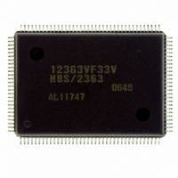
Manufacturer Part Number
D12363VF33V
Description
IC H8S/2363 MCU ROMLESS 128QFP
Manufacturer
Renesas Electronics America
Series
H8® H8S/2300r
Specifications of D12363VF33V
Core Processor
H8S/2000
Core Size
16-Bit
Speed
33MHz
Connectivity
I²C, IrDA, SCI, SmartCard
Peripherals
DMA, POR, PWM, WDT
Number Of I /o
84
Program Memory Type
ROMless
Ram Size
16K x 8
Voltage - Supply (vcc/vdd)
3 V ~ 3.6 V
Data Converters
A/D 10x10b, D/A 2x8b
Oscillator Type
Internal
Operating Temperature
-20°C ~ 75°C
Package / Case
128-QFP
For Use With
YR0K42378FC000BA - KIT EVAL FOR H8S/2378
Lead Free Status / RoHS Status
Lead free / RoHS Compliant
Eeprom Size
-
Program Memory Size
-
Available stocks
Company
Part Number
Manufacturer
Quantity
Price
Company:

Part Number:
D12363VF33V
Manufacturer:
ST
Quantity:
67 000
Company:
Part Number:
D12363VF33V
Manufacturer:
Renesas Electronics America
Quantity:
10 000
Part Number:
D12363VF33V
Manufacturer:
RENSAS
Quantity:
20 000


A single divided block is erased by one erasing processing. For block divisions, refer to figure
20.4. To erase two or more blocks, update the erase block number and perform the erasing
processing for each block.
1. Select the on-chip program to be downloaded
2. Set the FEBS parameter necessary for erasure
3. Erasure
4. The return value in the erasing program, FPFR (general register R0L) is determined.
5. Determine whether erasure of the necessary blocks has completed.
Set the EPVB bit in FECS to 1.
Several programming/erasing programs cannot be selected at one time. If several programs are
set, download is not performed and a download error is reported to the SS bit in the DPFR
parameter.
Specify the start address of a download destination by FTDAR.
The procedures to be carried out after setting FKEY, e.g. download and initialization, are the
same as those in the programming procedure. For details, refer to Programming Procedure in
User Program Mode in section 20.4.2 (2) Programming Procedure in User Program Mode.
The procedures after setting parameters for erasing programs are as follows:
Set the erase block number of the user MAT in the flash erase block select parameter FEBS
(general register ER0). If a value other than an erase block number of the user MAT is set, no
block is erased even though the erasing program is executed, and an error is returned to the
return value parameter FPFR.
Similar to as in programming, there is an entry point of the erasing program in the area from
the start address of a download destination specified by FTDAR + 16 bytes of on-chip RAM.
The subroutine is called and erasing is executed by using the following steps.
MOV.L
JSR
NOP
•
•
•
If more than one block is to be erased, update the FEBS parameter and repeat steps 3 to 5.
Blocks that have already been erased can be erased again.
The general registers other than ER0, ER1 are held in the erasing program.
R0L is a return value of the FPFR parameter.
Since the stack area is used in the erasing program, a stack area of a maximum 128 bytes
must be allocated in RAM
#DLTOP+16,ER2;
@ER2;
Set entry address to ER2
Call erasing routine
Section 20 Flash Memory (0.18-μm F-ZTAT Version)
Rev.6.00 Mar. 18, 2009 Page 763 of 980
REJ09B0050-0600
Related parts for D12363VF33V
Image
Part Number
Description
Manufacturer
Datasheet
Request
R

Part Number:
Description:
KIT STARTER FOR M16C/29
Manufacturer:
Renesas Electronics America
Datasheet:

Part Number:
Description:
KIT STARTER FOR R8C/2D
Manufacturer:
Renesas Electronics America
Datasheet:

Part Number:
Description:
R0K33062P STARTER KIT
Manufacturer:
Renesas Electronics America
Datasheet:

Part Number:
Description:
KIT STARTER FOR R8C/23 E8A
Manufacturer:
Renesas Electronics America
Datasheet:

Part Number:
Description:
KIT STARTER FOR R8C/25
Manufacturer:
Renesas Electronics America
Datasheet:

Part Number:
Description:
KIT STARTER H8S2456 SHARPE DSPLY
Manufacturer:
Renesas Electronics America
Datasheet:

Part Number:
Description:
KIT STARTER FOR R8C38C
Manufacturer:
Renesas Electronics America
Datasheet:

Part Number:
Description:
KIT STARTER FOR R8C35C
Manufacturer:
Renesas Electronics America
Datasheet:

Part Number:
Description:
KIT STARTER FOR R8CL3AC+LCD APPS
Manufacturer:
Renesas Electronics America
Datasheet:
Part Number:
Description:
KIT STARTER FOR RX610
Manufacturer:
Renesas Electronics America
Datasheet:

Part Number:
Description:
KIT STARTER FOR R32C/118
Manufacturer:
Renesas Electronics America
Datasheet:

Part Number:
Description:
KIT DEV RSK-R8C/26-29
Manufacturer:
Renesas Electronics America
Datasheet:

Part Number:
Description:
KIT STARTER FOR SH7124
Manufacturer:
Renesas Electronics America
Datasheet:

Part Number:
Description:
KIT STARTER FOR H8SX/1622
Manufacturer:
Renesas Electronics America
Datasheet:

Part Number:
Description:
KIT DEV FOR SH7203
Manufacturer:
Renesas Electronics America
Datasheet: