D12363VF33V Renesas Electronics America, D12363VF33V Datasheet - Page 418
D12363VF33V
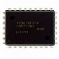
Manufacturer Part Number
D12363VF33V
Description
IC H8S/2363 MCU ROMLESS 128QFP
Manufacturer
Renesas Electronics America
Series
H8® H8S/2300r
Specifications of D12363VF33V
Core Processor
H8S/2000
Core Size
16-Bit
Speed
33MHz
Connectivity
I²C, IrDA, SCI, SmartCard
Peripherals
DMA, POR, PWM, WDT
Number Of I /o
84
Program Memory Type
ROMless
Ram Size
16K x 8
Voltage - Supply (vcc/vdd)
3 V ~ 3.6 V
Data Converters
A/D 10x10b, D/A 2x8b
Oscillator Type
Internal
Operating Temperature
-20°C ~ 75°C
Package / Case
128-QFP
For Use With
YR0K42378FC000BA - KIT EVAL FOR H8S/2378
Lead Free Status / RoHS Status
Lead free / RoHS Compliant
Eeprom Size
-
Program Memory Size
-
Available stocks
Company
Part Number
Manufacturer
Quantity
Price
Company:

Part Number:
D12363VF33V
Manufacturer:
ST
Quantity:
67 000
Company:
Part Number:
D12363VF33V
Manufacturer:
Renesas Electronics America
Quantity:
10 000
Part Number:
D12363VF33V
Manufacturer:
RENSAS
Quantity:
20 000


Section 9 I/O Ports
9.5.3
PORT5 shows the pin states. PORT5 cannot be modified.
Note:
9.5.4
Port 5 pins also function as the pins for SCI I/Os, A/D converter inputs, and interrupt inputs. The
correspondence between the register specification and the pin functions is shown below.
•
The pin function is switched as shown below according to the combination of bits TRGS1 and
TRGS0 in the A/D control register (ADCR), bit ITS3 in ITSR, and bit P53DDR.
Notes: 1. ADTRG input when TRGS1 = TRGS0 = 1.
Rev.6.00 Mar. 18, 2009 Page 358 of 980
REJ09B0050-0600
P53DDR
Pin function
Bit
7
to
4
3
2
1
0
P53/ADTRG/IRQ3
*
2. IRQ3 input when ITS3 = 0.
Bit Name
—
P53
P52
P51
P50
Port 5 Register (PORT5)
Pin Functions
Determined by the states of pins P53 to P50.
Initial Value
Undefined
— *
— *
— *
— *
P53 input
0
R/W
R
R
R
R
R
Description
Reserved
Undefined values are read from these bits.
If bits P53 to P50 are read while P5DDR bits are set
to 1, the P5DR values are read. If a port 5 read is
performed while P5DDR bits are cleared to 0, the
pin states are read.
IRQ3 interrupt input *
ADTRG input *
1
2
P53 output
1
Related parts for D12363VF33V
Image
Part Number
Description
Manufacturer
Datasheet
Request
R

Part Number:
Description:
KIT STARTER FOR M16C/29
Manufacturer:
Renesas Electronics America
Datasheet:

Part Number:
Description:
KIT STARTER FOR R8C/2D
Manufacturer:
Renesas Electronics America
Datasheet:

Part Number:
Description:
R0K33062P STARTER KIT
Manufacturer:
Renesas Electronics America
Datasheet:

Part Number:
Description:
KIT STARTER FOR R8C/23 E8A
Manufacturer:
Renesas Electronics America
Datasheet:

Part Number:
Description:
KIT STARTER FOR R8C/25
Manufacturer:
Renesas Electronics America
Datasheet:

Part Number:
Description:
KIT STARTER H8S2456 SHARPE DSPLY
Manufacturer:
Renesas Electronics America
Datasheet:

Part Number:
Description:
KIT STARTER FOR R8C38C
Manufacturer:
Renesas Electronics America
Datasheet:

Part Number:
Description:
KIT STARTER FOR R8C35C
Manufacturer:
Renesas Electronics America
Datasheet:

Part Number:
Description:
KIT STARTER FOR R8CL3AC+LCD APPS
Manufacturer:
Renesas Electronics America
Datasheet:
Part Number:
Description:
KIT STARTER FOR RX610
Manufacturer:
Renesas Electronics America
Datasheet:

Part Number:
Description:
KIT STARTER FOR R32C/118
Manufacturer:
Renesas Electronics America
Datasheet:

Part Number:
Description:
KIT DEV RSK-R8C/26-29
Manufacturer:
Renesas Electronics America
Datasheet:

Part Number:
Description:
KIT STARTER FOR SH7124
Manufacturer:
Renesas Electronics America
Datasheet:

Part Number:
Description:
KIT STARTER FOR H8SX/1622
Manufacturer:
Renesas Electronics America
Datasheet:

Part Number:
Description:
KIT DEV FOR SH7203
Manufacturer:
Renesas Electronics America
Datasheet: