D12363VF33V Renesas Electronics America, D12363VF33V Datasheet - Page 349
D12363VF33V
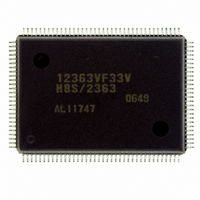
Manufacturer Part Number
D12363VF33V
Description
IC H8S/2363 MCU ROMLESS 128QFP
Manufacturer
Renesas Electronics America
Series
H8® H8S/2300r
Specifications of D12363VF33V
Core Processor
H8S/2000
Core Size
16-Bit
Speed
33MHz
Connectivity
I²C, IrDA, SCI, SmartCard
Peripherals
DMA, POR, PWM, WDT
Number Of I /o
84
Program Memory Type
ROMless
Ram Size
16K x 8
Voltage - Supply (vcc/vdd)
3 V ~ 3.6 V
Data Converters
A/D 10x10b, D/A 2x8b
Oscillator Type
Internal
Operating Temperature
-20°C ~ 75°C
Package / Case
128-QFP
For Use With
YR0K42378FC000BA - KIT EVAL FOR H8S/2378
Lead Free Status / RoHS Status
Lead free / RoHS Compliant
Eeprom Size
-
Program Memory Size
-
Available stocks
Company
Part Number
Manufacturer
Quantity
Price
Company:

Part Number:
D12363VF33V
Manufacturer:
ST
Quantity:
67 000
Company:
Part Number:
D12363VF33V
Manufacturer:
Renesas Electronics America
Quantity:
10 000
Part Number:
D12363VF33V
Manufacturer:
RENSAS
Quantity:
20 000


• If a DMAC transfer cycle occurs immediately after a DMAC register read cycle, the DMAC
7.7.2
When the MSTP13 bit in MSTPCRH is set to 1, the DMAC clock stops, and the module stop state
is entered. However, 1 cannot be written to the MSTP13 bit if any of the DMAC channels is
enabled. This setting should therefore be made when DMAC operation is stopped.
When the DMAC clock stops, DMAC register accesses can no longer be made. Since the
following DMAC register settings are valid even in the module stop state, they should be
invalidated, if necessary, before a module stop.
• Transfer end/break interrupt (DTE = 0 and DTIE = 1)
• TEND pin enable (TEE = 1)
• DACK pin enable (FAE = 0 and SAE = 1)
7.7.3
When the WDBE bit of BCR in the bus controller is set to 1, enabling the write data buffer
function, external write cycles in dual address transfers or single address transfers are executed in
parallel with internal accesses (on-chip memory or internal I/O registers).
register is read as shown in figure 7.40.
DMA internal
address
DMA register
operation
Module Stop
Write Data Buffer Function
DMA control
Figure 7.40 Contention between DMAC Register Update and CPU Read
Note: The lower word of MAR is the updated value after the operation in [1].
MAR upper
word read
Idle
CPU longword read
[1]
MAR lower
word read
Transfe
source
Read
Rev.6.00 Mar. 18, 2009 Page 289 of 980
[2]
DMA read
destination
DMA transfer cycle
Transfer
Write
Section 7 DMA Controller (DMAC)
DMA write
Idle
REJ09B0050-0600
Related parts for D12363VF33V
Image
Part Number
Description
Manufacturer
Datasheet
Request
R

Part Number:
Description:
KIT STARTER FOR M16C/29
Manufacturer:
Renesas Electronics America
Datasheet:

Part Number:
Description:
KIT STARTER FOR R8C/2D
Manufacturer:
Renesas Electronics America
Datasheet:

Part Number:
Description:
R0K33062P STARTER KIT
Manufacturer:
Renesas Electronics America
Datasheet:

Part Number:
Description:
KIT STARTER FOR R8C/23 E8A
Manufacturer:
Renesas Electronics America
Datasheet:

Part Number:
Description:
KIT STARTER FOR R8C/25
Manufacturer:
Renesas Electronics America
Datasheet:

Part Number:
Description:
KIT STARTER H8S2456 SHARPE DSPLY
Manufacturer:
Renesas Electronics America
Datasheet:

Part Number:
Description:
KIT STARTER FOR R8C38C
Manufacturer:
Renesas Electronics America
Datasheet:

Part Number:
Description:
KIT STARTER FOR R8C35C
Manufacturer:
Renesas Electronics America
Datasheet:

Part Number:
Description:
KIT STARTER FOR R8CL3AC+LCD APPS
Manufacturer:
Renesas Electronics America
Datasheet:
Part Number:
Description:
KIT STARTER FOR RX610
Manufacturer:
Renesas Electronics America
Datasheet:

Part Number:
Description:
KIT STARTER FOR R32C/118
Manufacturer:
Renesas Electronics America
Datasheet:

Part Number:
Description:
KIT DEV RSK-R8C/26-29
Manufacturer:
Renesas Electronics America
Datasheet:

Part Number:
Description:
KIT STARTER FOR SH7124
Manufacturer:
Renesas Electronics America
Datasheet:

Part Number:
Description:
KIT STARTER FOR H8SX/1622
Manufacturer:
Renesas Electronics America
Datasheet:

Part Number:
Description:
KIT DEV FOR SH7203
Manufacturer:
Renesas Electronics America
Datasheet: