D12363VF33V Renesas Electronics America, D12363VF33V Datasheet - Page 76
D12363VF33V
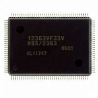
Manufacturer Part Number
D12363VF33V
Description
IC H8S/2363 MCU ROMLESS 128QFP
Manufacturer
Renesas Electronics America
Series
H8® H8S/2300r
Specifications of D12363VF33V
Core Processor
H8S/2000
Core Size
16-Bit
Speed
33MHz
Connectivity
I²C, IrDA, SCI, SmartCard
Peripherals
DMA, POR, PWM, WDT
Number Of I /o
84
Program Memory Type
ROMless
Ram Size
16K x 8
Voltage - Supply (vcc/vdd)
3 V ~ 3.6 V
Data Converters
A/D 10x10b, D/A 2x8b
Oscillator Type
Internal
Operating Temperature
-20°C ~ 75°C
Package / Case
128-QFP
For Use With
YR0K42378FC000BA - KIT EVAL FOR H8S/2378
Lead Free Status / RoHS Status
Lead free / RoHS Compliant
Eeprom Size
-
Program Memory Size
-
Available stocks
Company
Part Number
Manufacturer
Quantity
Price
Company:

Part Number:
D12363VF33V
Manufacturer:
ST
Quantity:
67 000
Company:
Part Number:
D12363VF33V
Manufacturer:
Renesas Electronics America
Quantity:
10 000
Part Number:
D12363VF33V
Manufacturer:
RENSAS
Quantity:
20 000


Section 1 Overview
Bus control
DMA controller
(DMAC)
Rev.6.00 Mar. 18, 2009 Page 16 of 980
REJ09B0050-0600
Type
Interrupt
signals
BACK
UCAS
LCAS
RAS2
RAS3
WAIT
OE
(OE)
DREQ1
DREQ0
TEND1,
TEND0
DACK1,
DACK0
Symbol
NMI
IRQ7 to
IRQ0
(IRQ7) to
(IRQ0)
Pin No.
TFP-120
107
70
71
91
92
69
69,
113
35,
34
37,
36
39,
38
32
29 to 26,
112 to 109,
102 to 95
117
78
79
101
102
77
77,
123
41,
40
43,
42
45,
44
38
33 to 30,
122 to 119,
112 to 105
QFP-128 *
1
Output Upper column address strobe
Output Lower column address strobe
Output Row address strobe signal for the
Input
Output Output enable signal for accessing
Input
Output These signals indicate the end of
Output DMAC single address transfer
I/O
Output Indicates the bus is released to the
Input
Input
external bus master.
signal for accessing the 16-bit
DRAM space.
Column address strobe signal for
accessing the 8-bit DRAM space.
signal for accessing the 16-bit
DRAM space.
DRAM interface.
Requests insertion of a wait state in
the bus cycle when accessing
external 3-state address space.
the DRAM space.
The output pins of OE and (OE) are
selected by the port function control
register 2 (PFCR2) of port 3.
These signals request DMAC
activation.
DMAC data transfer.
acknowledge signals.
Function
Nonmaskable interrupt request pin.
Fix high when not used.
These pins request a maskable
interrupt.
The input pins of IRQn and (IRQn)
are selected by the IRQ pin select
register (ITSR) of the interrupt
controller. (n = 0 to 7)
Related parts for D12363VF33V
Image
Part Number
Description
Manufacturer
Datasheet
Request
R

Part Number:
Description:
KIT STARTER FOR M16C/29
Manufacturer:
Renesas Electronics America
Datasheet:

Part Number:
Description:
KIT STARTER FOR R8C/2D
Manufacturer:
Renesas Electronics America
Datasheet:

Part Number:
Description:
R0K33062P STARTER KIT
Manufacturer:
Renesas Electronics America
Datasheet:

Part Number:
Description:
KIT STARTER FOR R8C/23 E8A
Manufacturer:
Renesas Electronics America
Datasheet:

Part Number:
Description:
KIT STARTER FOR R8C/25
Manufacturer:
Renesas Electronics America
Datasheet:

Part Number:
Description:
KIT STARTER H8S2456 SHARPE DSPLY
Manufacturer:
Renesas Electronics America
Datasheet:

Part Number:
Description:
KIT STARTER FOR R8C38C
Manufacturer:
Renesas Electronics America
Datasheet:

Part Number:
Description:
KIT STARTER FOR R8C35C
Manufacturer:
Renesas Electronics America
Datasheet:

Part Number:
Description:
KIT STARTER FOR R8CL3AC+LCD APPS
Manufacturer:
Renesas Electronics America
Datasheet:
Part Number:
Description:
KIT STARTER FOR RX610
Manufacturer:
Renesas Electronics America
Datasheet:

Part Number:
Description:
KIT STARTER FOR R32C/118
Manufacturer:
Renesas Electronics America
Datasheet:

Part Number:
Description:
KIT DEV RSK-R8C/26-29
Manufacturer:
Renesas Electronics America
Datasheet:

Part Number:
Description:
KIT STARTER FOR SH7124
Manufacturer:
Renesas Electronics America
Datasheet:

Part Number:
Description:
KIT STARTER FOR H8SX/1622
Manufacturer:
Renesas Electronics America
Datasheet:

Part Number:
Description:
KIT DEV FOR SH7203
Manufacturer:
Renesas Electronics America
Datasheet: