D12363VF33V Renesas Electronics America, D12363VF33V Datasheet - Page 56
D12363VF33V
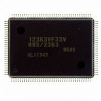
Manufacturer Part Number
D12363VF33V
Description
IC H8S/2363 MCU ROMLESS 128QFP
Manufacturer
Renesas Electronics America
Series
H8® H8S/2300r
Specifications of D12363VF33V
Core Processor
H8S/2000
Core Size
16-Bit
Speed
33MHz
Connectivity
I²C, IrDA, SCI, SmartCard
Peripherals
DMA, POR, PWM, WDT
Number Of I /o
84
Program Memory Type
ROMless
Ram Size
16K x 8
Voltage - Supply (vcc/vdd)
3 V ~ 3.6 V
Data Converters
A/D 10x10b, D/A 2x8b
Oscillator Type
Internal
Operating Temperature
-20°C ~ 75°C
Package / Case
128-QFP
For Use With
YR0K42378FC000BA - KIT EVAL FOR H8S/2378
Lead Free Status / RoHS Status
Lead free / RoHS Compliant
Eeprom Size
-
Program Memory Size
-
Available stocks
Company
Part Number
Manufacturer
Quantity
Price
Company:

Part Number:
D12363VF33V
Manufacturer:
ST
Quantity:
67 000
Company:
Part Number:
D12363VF33V
Manufacturer:
Renesas Electronics America
Quantity:
10 000
Part Number:
D12363VF33V
Manufacturer:
RENSAS
Quantity:
20 000


Section 11 Programmable Pulse Generator (PPG)
Table 11.1
Section 12 8-Bit Timers (TMR)
Table 12.1
Table 12.2
Table 12.3
Table 12.4
Table 12.5
Section 13 Watchdog Timer
Table 13.1
Table 13.2
Section 14 Serial Communication Interface (SCI, IrDA)
Table 14.1
Table 14.2
Table 14.3
Table 14.4
Table 14.5
Table 14.6
Table 14.7
Table 14.8
Table 14.9
Table 14.10 Serial Transfer Formats (Asynchronous Mode) ..................................................... 577
Table 14.11 SSR Status Flags and Receive Data Handling........................................................ 585
Table 14.12 Settings of Bits IrCKS2 to IrCKS0 ........................................................................ 618
Table 14.13 SCI Interrupt Sources ............................................................................................. 620
Table 14.14 Interrupt Sources .................................................................................................... 621
Section 15 I
Table 15.1
Table 15.2
Table 15.3
Table 15.4
Section 16 A/D Converter
Table 16.1
Rev.6.00 Mar. 18, 2009 Page liv of lviii
REJ09B0050-0600
Pin Configuration ................................................................................................... 487
Pin Configuration ................................................................................................... 509
Clock Input to TCNT and Count Condition ........................................................... 512
8-Bit Timer Interrupt Sources ................................................................................ 521
Timer Output Priorities .......................................................................................... 525
Switching of Internal Clock and TCNT Operation ................................................ 526
Pin Configuration ................................................................................................... 530
WDT Interrupt Source............................................................................................ 536
Pin Configuration ................................................................................................... 544
Relationships between N Setting in BRR and Bit Rate B ...................................... 564
BRR Settings for Various Bit Rates (Asynchronous Mode) .................................. 565
Maximum Bit Rate for Each Frequency (Asynchronous Mode)............................ 567
Maximum Bit Rate with External Clock Input (Asynchronous Mode).................. 568
BRR Settings for Various Bit Rates (Clocked Synchronous Mode) ...................... 569
Maximum Bit Rate with External Clock Input (Clocked Synchronous Mode)...... 570
Examples of Bit Rate for Various BRR Settings (Smart Card Interface Mode)
(when n = 0 and S = 372) ....................................................................................... 571
Maximum Bit Rate at Various Frequencies (Smart Card Interface Mode)
(when S = 372) ....................................................................................................... 572
Pin Configuration ................................................................................................... 631
Transfer Rate.......................................................................................................... 634
Interrupt Requests .................................................................................................. 658
Time for monitoring SCL....................................................................................... 659
Pin Configuration ................................................................................................... 663
2
C Bus Interface2 (IIC2) (Option)
Related parts for D12363VF33V
Image
Part Number
Description
Manufacturer
Datasheet
Request
R

Part Number:
Description:
KIT STARTER FOR M16C/29
Manufacturer:
Renesas Electronics America
Datasheet:

Part Number:
Description:
KIT STARTER FOR R8C/2D
Manufacturer:
Renesas Electronics America
Datasheet:

Part Number:
Description:
R0K33062P STARTER KIT
Manufacturer:
Renesas Electronics America
Datasheet:

Part Number:
Description:
KIT STARTER FOR R8C/23 E8A
Manufacturer:
Renesas Electronics America
Datasheet:

Part Number:
Description:
KIT STARTER FOR R8C/25
Manufacturer:
Renesas Electronics America
Datasheet:

Part Number:
Description:
KIT STARTER H8S2456 SHARPE DSPLY
Manufacturer:
Renesas Electronics America
Datasheet:

Part Number:
Description:
KIT STARTER FOR R8C38C
Manufacturer:
Renesas Electronics America
Datasheet:

Part Number:
Description:
KIT STARTER FOR R8C35C
Manufacturer:
Renesas Electronics America
Datasheet:

Part Number:
Description:
KIT STARTER FOR R8CL3AC+LCD APPS
Manufacturer:
Renesas Electronics America
Datasheet:
Part Number:
Description:
KIT STARTER FOR RX610
Manufacturer:
Renesas Electronics America
Datasheet:

Part Number:
Description:
KIT STARTER FOR R32C/118
Manufacturer:
Renesas Electronics America
Datasheet:

Part Number:
Description:
KIT DEV RSK-R8C/26-29
Manufacturer:
Renesas Electronics America
Datasheet:

Part Number:
Description:
KIT STARTER FOR SH7124
Manufacturer:
Renesas Electronics America
Datasheet:

Part Number:
Description:
KIT STARTER FOR H8SX/1622
Manufacturer:
Renesas Electronics America
Datasheet:

Part Number:
Description:
KIT DEV FOR SH7203
Manufacturer:
Renesas Electronics America
Datasheet: