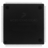
MC9S12XA512CAG Freescale Semiconductor, MC9S12XA512CAG Datasheet - Page 209

MC9S12XA512CAG
Manufacturer Part Number
MC9S12XA512CAG
Description
IC MCU 512K FLASH 144-LQFP
Manufacturer
Freescale Semiconductor
Series
HCS12r
Specifications of MC9S12XA512CAG
Core Processor
HCS12X
Core Size
16-Bit
Speed
80MHz
Connectivity
EBI/EMI, I²C, IrDA, LIN, SCI, SPI
Peripherals
LVD, POR, PWM, WDT
Number Of I /o
119
Program Memory Size
512KB (512K x 8)
Program Memory Type
FLASH
Eeprom Size
4K x 8
Ram Size
32K x 8
Voltage - Supply (vcc/vdd)
2.35 V ~ 5.5 V
Data Converters
A/D 24x10b
Oscillator Type
External
Operating Temperature
-40°C ~ 85°C
Package / Case
144-LQFP
Processor Series
S12XA
Core
HCS12
Data Bus Width
16 bit
Data Ram Size
32 KB
Interface Type
CAN, I2C, SCI, SPI
Maximum Clock Frequency
40 MHz
Number Of Programmable I/os
119
Number Of Timers
12
Maximum Operating Temperature
+ 85 C
Mounting Style
SMD/SMT
3rd Party Development Tools
EWHCS12
Development Tools By Supplier
EVB9S12XDP512E
Minimum Operating Temperature
- 40 C
On-chip Adc
2 (10 bit, 24 Channel)
Lead Free Status / RoHS Status
Lead free / RoHS Compliant
Available stocks
Company
Part Number
Manufacturer
Quantity
Price
Company:
Part Number:
MC9S12XA512CAG
Manufacturer:
Freescale
Quantity:
490
Company:
Part Number:
MC9S12XA512CAG
Manufacturer:
Freescale Semiconductor
Quantity:
10 000
- Current page: 209 of 1348
- Download datasheet (8Mb)
6.8.1.1
6.8.1.2
Instructions that use this addressing mode either have no operands or all operands are in internal XGATE
registers:.
Examples
6.8.1.3
Operands for immediate mode instructions are included in the instruction stream and are fetched into the
instruction queue along with the rest of the 16 bit instruction. The ’#’ symbol is used to indicate an
immediate addressing mode operand. This address mode is used for semaphore instructions.
Examples:
Freescale Semiconductor
RD
RD.L
RD.H
RS, RS1, RS2
RS.L, RS1.L, RS2.L
RS.H, RS1.H, RS2.H
RB
RI
RI+
–RI
BRK
RTS
CSEM
SSEM
Naming Conventions
Inherent Addressing Mode (INH)
Immediate 3-Bit Wide (IMM3)
Even though register R1 is intended to be used as a pointer to the variable
segment, it may be used as a general purpose data register as well.
Selecting R0 as destination register will discard the result of the instruction.
Only the condition code register will be updated
#1
#3
; Unlock semaphore 1
; Lock Semaphore 3
Destination register, allowed range is R0–R7
Low byte of the destination register, bits [7:0]
High byte of the destination register, bits [15:8]
Source register, allowed range is R0–R7
Low byte of the source register, bits [7:0]
High byte of the source register, bits[15:8]
Base register for indexed addressing modes, allowed
range is R0–R7
Offset register for indexed addressing modes with
register offset, allowed range is R0–R7
Offset register for indexed addressing modes with
register offset and post-increment,
Allowed range is R0–R7 (R0+ is equivalent to R0)
Offset register for indexed addressing modes with
register offset and pre-decrement,
Allowed range is R0–R7 (–R0 is equivalent to R0)
MC9S12XDP512 Data Sheet, Rev. 2.21
NOTE
Chapter 6 XGATE (S12XGATEV2)
209
Related parts for MC9S12XA512CAG
Image
Part Number
Description
Manufacturer
Datasheet
Request
R
Part Number:
Description:
Manufacturer:
Freescale Semiconductor, Inc
Datasheet:
Part Number:
Description:
Manufacturer:
Freescale Semiconductor, Inc
Datasheet:
Part Number:
Description:
Manufacturer:
Freescale Semiconductor, Inc
Datasheet:
Part Number:
Description:
Manufacturer:
Freescale Semiconductor, Inc
Datasheet:
Part Number:
Description:
Manufacturer:
Freescale Semiconductor, Inc
Datasheet:
Part Number:
Description:
Manufacturer:
Freescale Semiconductor, Inc
Datasheet:
Part Number:
Description:
Manufacturer:
Freescale Semiconductor, Inc
Datasheet:
Part Number:
Description:
Manufacturer:
Freescale Semiconductor, Inc
Datasheet:
Part Number:
Description:
Manufacturer:
Freescale Semiconductor, Inc
Datasheet:
Part Number:
Description:
Manufacturer:
Freescale Semiconductor, Inc
Datasheet:
Part Number:
Description:
Manufacturer:
Freescale Semiconductor, Inc
Datasheet:
Part Number:
Description:
Manufacturer:
Freescale Semiconductor, Inc
Datasheet:
Part Number:
Description:
Manufacturer:
Freescale Semiconductor, Inc
Datasheet:
Part Number:
Description:
Manufacturer:
Freescale Semiconductor, Inc
Datasheet:
Part Number:
Description:
Manufacturer:
Freescale Semiconductor, Inc
Datasheet:


