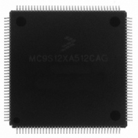
MC9S12XA512CAG Freescale Semiconductor, MC9S12XA512CAG Datasheet - Page 167

MC9S12XA512CAG
Manufacturer Part Number
MC9S12XA512CAG
Description
IC MCU 512K FLASH 144-LQFP
Manufacturer
Freescale Semiconductor
Series
HCS12r
Specifications of MC9S12XA512CAG
Core Processor
HCS12X
Core Size
16-Bit
Speed
80MHz
Connectivity
EBI/EMI, I²C, IrDA, LIN, SCI, SPI
Peripherals
LVD, POR, PWM, WDT
Number Of I /o
119
Program Memory Size
512KB (512K x 8)
Program Memory Type
FLASH
Eeprom Size
4K x 8
Ram Size
32K x 8
Voltage - Supply (vcc/vdd)
2.35 V ~ 5.5 V
Data Converters
A/D 24x10b
Oscillator Type
External
Operating Temperature
-40°C ~ 85°C
Package / Case
144-LQFP
Processor Series
S12XA
Core
HCS12
Data Bus Width
16 bit
Data Ram Size
32 KB
Interface Type
CAN, I2C, SCI, SPI
Maximum Clock Frequency
40 MHz
Number Of Programmable I/os
119
Number Of Timers
12
Maximum Operating Temperature
+ 85 C
Mounting Style
SMD/SMT
3rd Party Development Tools
EWHCS12
Development Tools By Supplier
EVB9S12XDP512E
Minimum Operating Temperature
- 40 C
On-chip Adc
2 (10 bit, 24 Channel)
Lead Free Status / RoHS Status
Lead free / RoHS Compliant
Available stocks
Company
Part Number
Manufacturer
Quantity
Price
Company:
Part Number:
MC9S12XA512CAG
Manufacturer:
Freescale
Quantity:
490
Company:
Part Number:
MC9S12XA512CAG
Manufacturer:
Freescale Semiconductor
Quantity:
10 000
- Current page: 167 of 1348
- Download datasheet (8Mb)
5.3.2.2
Writes to this register will abort current conversion sequence but will not start a new sequence.
Read: Anytime
Write: Anytime
Freescale Semiconductor
ETRIGCH[2:0]
ETRIGSEL
Reset
Field
2–0
W
7
R
ETRIGSEL
ATD Control Register 1 (ATDCTL1)
1
0
7
External Trigger Source Select — This bit selects the external trigger source to be either one of the AD
channels or one of the ETRIG3–0 inputs. See the device overview chapter for availability and connectivity of
ETRIG3–0 inputs. If ETRIG3–0 input option is not available, writing a 1 to ETRISEL only sets the bit but has
not effect, that means still one of the AD channels (selected by ETRIGCH2–0) is the source for external trigger.
The coding is summarized in
External Trigger Channel Select — These bits select one of the AD channels or one of the ETRIG3–0 inputs
as source for the external trigger. The coding is summarized in
ETRIGSEL
Only if ETRIG3–0 input option is available (see device overview chapter), else ETRISEL is
ignored, that means external trigger source is still on one of the AD channels selected by
ETRIGCH2–0
0
0
0
0
0
0
0
0
1
1
1
1
1
= Unimplemented or Reserved
0
0
6
ETRIGCH2
Table 5-4. External Trigger Channel Select Coding
Figure 5-4. ATD Control Register 1 (ATDCTL1)
0
0
0
0
1
1
1
1
0
0
0
0
1
Table 5-3. ATDCTL1 Field Descriptions
MC9S12XDP512 Data Sheet, Rev. 2.21
0
0
5
Table
ETRIGCH1
X
0
0
1
1
0
0
1
1
0
0
1
1
5-4.
0
0
4
ETRIGCH0
Description
X
0
1
0
1
0
1
0
1
0
1
0
1
Chapter 5 Analog-to-Digital Converter (S12ATD10B8CV2)
0
0
3
External trigger source is
Table
ETRIGCH2
5-4.
Reserved
ETRIG0
ETRIG1
ETRIG2
ETRIG3
1
2
AN0
AN1
AN2
AN3
AN4
AN5
AN6
AN7
1
1
1
1
ETRIGCH1
1
1
ETRIGCH0
1
0
167
Related parts for MC9S12XA512CAG
Image
Part Number
Description
Manufacturer
Datasheet
Request
R
Part Number:
Description:
Manufacturer:
Freescale Semiconductor, Inc
Datasheet:
Part Number:
Description:
Manufacturer:
Freescale Semiconductor, Inc
Datasheet:
Part Number:
Description:
Manufacturer:
Freescale Semiconductor, Inc
Datasheet:
Part Number:
Description:
Manufacturer:
Freescale Semiconductor, Inc
Datasheet:
Part Number:
Description:
Manufacturer:
Freescale Semiconductor, Inc
Datasheet:
Part Number:
Description:
Manufacturer:
Freescale Semiconductor, Inc
Datasheet:
Part Number:
Description:
Manufacturer:
Freescale Semiconductor, Inc
Datasheet:
Part Number:
Description:
Manufacturer:
Freescale Semiconductor, Inc
Datasheet:
Part Number:
Description:
Manufacturer:
Freescale Semiconductor, Inc
Datasheet:
Part Number:
Description:
Manufacturer:
Freescale Semiconductor, Inc
Datasheet:
Part Number:
Description:
Manufacturer:
Freescale Semiconductor, Inc
Datasheet:
Part Number:
Description:
Manufacturer:
Freescale Semiconductor, Inc
Datasheet:
Part Number:
Description:
Manufacturer:
Freescale Semiconductor, Inc
Datasheet:
Part Number:
Description:
Manufacturer:
Freescale Semiconductor, Inc
Datasheet:
Part Number:
Description:
Manufacturer:
Freescale Semiconductor, Inc
Datasheet:


