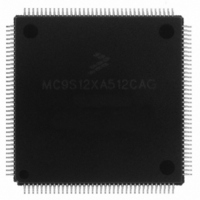
MC9S12XA512CAG Freescale Semiconductor, MC9S12XA512CAG Datasheet - Page 1155

MC9S12XA512CAG
Manufacturer Part Number
MC9S12XA512CAG
Description
IC MCU 512K FLASH 144-LQFP
Manufacturer
Freescale Semiconductor
Series
HCS12r
Specifications of MC9S12XA512CAG
Core Processor
HCS12X
Core Size
16-Bit
Speed
80MHz
Connectivity
EBI/EMI, I²C, IrDA, LIN, SCI, SPI
Peripherals
LVD, POR, PWM, WDT
Number Of I /o
119
Program Memory Size
512KB (512K x 8)
Program Memory Type
FLASH
Eeprom Size
4K x 8
Ram Size
32K x 8
Voltage - Supply (vcc/vdd)
2.35 V ~ 5.5 V
Data Converters
A/D 24x10b
Oscillator Type
External
Operating Temperature
-40°C ~ 85°C
Package / Case
144-LQFP
Processor Series
S12XA
Core
HCS12
Data Bus Width
16 bit
Data Ram Size
32 KB
Interface Type
CAN, I2C, SCI, SPI
Maximum Clock Frequency
40 MHz
Number Of Programmable I/os
119
Number Of Timers
12
Maximum Operating Temperature
+ 85 C
Mounting Style
SMD/SMT
3rd Party Development Tools
EWHCS12
Development Tools By Supplier
EVB9S12XDP512E
Minimum Operating Temperature
- 40 C
On-chip Adc
2 (10 bit, 24 Channel)
Lead Free Status / RoHS Status
Lead free / RoHS Compliant
Available stocks
Company
Part Number
Manufacturer
Quantity
Price
Company:
Part Number:
MC9S12XA512CAG
Manufacturer:
Freescale
Quantity:
490
Company:
Part Number:
MC9S12XA512CAG
Manufacturer:
Freescale Semiconductor
Quantity:
10 000
- Current page: 1155 of 1348
- Download datasheet (8Mb)
CBEIE, CCIE and KEYACC bits are readable and writable while all remaining bits read 0 and are not
writable in normal mode. KEYACC is only writable if KEYEN (see
Register (FSEC)”
mass erase and erase verify operations. When writing to the FCNFG register in special mode, all
unimplemented/ reserved bits must be written to 0.
28.3.2.5
The FPROT register defines which Flash sectors are protected against program or erase operations.
Freescale Semiconductor
KEYACC
BKSEL
Reset
Reset
CBEIE
Field
CCIE
7
6
5
0
W
W
R
R
CBEIE
CBEIE
Command Buffer Empty Interrupt Enable — The CBEIE bit enables an interrupt in case of an empty command
buffer in the Flash module.
0 Command buffer empty interrupt disabled.
1 An interrupt will be requested whenever the CBEIF flag (see
Command Complete Interrupt Enable — The CCIE bit enables an interrupt in case all commands have been
completed in the Flash module.
0 Command complete interrupt disabled.
1 An interrupt will be requested whenever the CCIF flag (see
Enable Security Key Writing
0 Flash writes are interpreted as the start of a command write sequence.
1 Writes to Flash array are interpreted as keys to open the backdoor. Reads of the Flash array return invalid
Block Select — The BKSEL bit indicates which register bank is active.
0 Select register bank associated with Flash block 0.
1 Select register bank associated with Flash block 1.
Flash Protection Register (FPROT)
0
0
7
7
(FSTAT)”)
is set.
data.
is set to the enabled state. BKSEL is readable and writable in special mode to simplify
Figure 28-8. Flash Configuration Register (FCNFG — Normal Mode)
Figure 28-9. Flash Configuration Register (FCNFG — Special Mode)
= Unimplemented or Reserved
= Unimplemented or Reserved
is set.
CCIE
CCIE
0
0
6
6
Table 28-8. FCNFG Field Descriptions
KEYACC
KEYACC
MC9S12XDP512 Data Sheet, Rev. 2.21
0
0
5
5
Undefined
Undefined
0
0
4
4
Description
Chapter 28 256 Kbyte Flash Module (S12XFTX256K2V1)
0
0
0
0
3
3
Section 28.3.2.6, “Flash Status Register
Section 28.3.2.6, “Flash Status Register
Section 28.3.2.2, “Flash Security
0
0
0
0
2
2
0
0
0
0
1
1
BKSEL
(FSTAT)”)
0
0
0
0
0
1157
Related parts for MC9S12XA512CAG
Image
Part Number
Description
Manufacturer
Datasheet
Request
R
Part Number:
Description:
Manufacturer:
Freescale Semiconductor, Inc
Datasheet:
Part Number:
Description:
Manufacturer:
Freescale Semiconductor, Inc
Datasheet:
Part Number:
Description:
Manufacturer:
Freescale Semiconductor, Inc
Datasheet:
Part Number:
Description:
Manufacturer:
Freescale Semiconductor, Inc
Datasheet:
Part Number:
Description:
Manufacturer:
Freescale Semiconductor, Inc
Datasheet:
Part Number:
Description:
Manufacturer:
Freescale Semiconductor, Inc
Datasheet:
Part Number:
Description:
Manufacturer:
Freescale Semiconductor, Inc
Datasheet:
Part Number:
Description:
Manufacturer:
Freescale Semiconductor, Inc
Datasheet:
Part Number:
Description:
Manufacturer:
Freescale Semiconductor, Inc
Datasheet:
Part Number:
Description:
Manufacturer:
Freescale Semiconductor, Inc
Datasheet:
Part Number:
Description:
Manufacturer:
Freescale Semiconductor, Inc
Datasheet:
Part Number:
Description:
Manufacturer:
Freescale Semiconductor, Inc
Datasheet:
Part Number:
Description:
Manufacturer:
Freescale Semiconductor, Inc
Datasheet:
Part Number:
Description:
Manufacturer:
Freescale Semiconductor, Inc
Datasheet:
Part Number:
Description:
Manufacturer:
Freescale Semiconductor, Inc
Datasheet:


