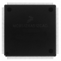
MC9S12XA512CAG Freescale Semiconductor, MC9S12XA512CAG Datasheet - Page 1169

MC9S12XA512CAG
Manufacturer Part Number
MC9S12XA512CAG
Description
IC MCU 512K FLASH 144-LQFP
Manufacturer
Freescale Semiconductor
Series
HCS12r
Specifications of MC9S12XA512CAG
Core Processor
HCS12X
Core Size
16-Bit
Speed
80MHz
Connectivity
EBI/EMI, I²C, IrDA, LIN, SCI, SPI
Peripherals
LVD, POR, PWM, WDT
Number Of I /o
119
Program Memory Size
512KB (512K x 8)
Program Memory Type
FLASH
Eeprom Size
4K x 8
Ram Size
32K x 8
Voltage - Supply (vcc/vdd)
2.35 V ~ 5.5 V
Data Converters
A/D 24x10b
Oscillator Type
External
Operating Temperature
-40°C ~ 85°C
Package / Case
144-LQFP
Processor Series
S12XA
Core
HCS12
Data Bus Width
16 bit
Data Ram Size
32 KB
Interface Type
CAN, I2C, SCI, SPI
Maximum Clock Frequency
40 MHz
Number Of Programmable I/os
119
Number Of Timers
12
Maximum Operating Temperature
+ 85 C
Mounting Style
SMD/SMT
3rd Party Development Tools
EWHCS12
Development Tools By Supplier
EVB9S12XDP512E
Minimum Operating Temperature
- 40 C
On-chip Adc
2 (10 bit, 24 Channel)
Lead Free Status / RoHS Status
Lead free / RoHS Compliant
Available stocks
Company
Part Number
Manufacturer
Quantity
Price
Company:
Part Number:
MC9S12XA512CAG
Manufacturer:
Freescale
Quantity:
490
Company:
Part Number:
MC9S12XA512CAG
Manufacturer:
Freescale Semiconductor
Quantity:
10 000
- Current page: 1169 of 1348
- Download datasheet (8Mb)
28.4.2.1
The erase verify operation will verify that a Flash block is erased.
An example flow to execute the erase verify operation is shown in
write sequence is as follows:
After launching the erase verify command, the CCIF flag in the FSTAT register will set after the operation
has completed unless a new command write sequence has been buffered. The number of bus cycles
required to execute the erase verify operation is equal to the number of addresses in a Flash block plus 14
bus cycles as measured from the time the CBEIF flag is cleared until the CCIF flag is set. Upon completion
of the erase verify operation, the BLANK flag in the FSTAT register will be set if all addresses in the
selected Flash blocks are verified to be erased. If any address in a selected Flash block is not erased, the
erase verify operation will terminate and the BLANK flag in the FSTAT register will remain clear. The
MRDS bits in the FTSTMOD register will determine the sense-amp margin setting during the erase verify
operation.
Freescale Semiconductor
1. Write to a Flash block address to start the command write sequence for the erase verify command.
2. Write the erase verify command, 0x05, to the FCMD register.
3. Clear the CBEIF flag in the FSTAT register by writing a 1 to CBEIF to launch the erase verify
The address and data written will be ignored. Multiple Flash blocks can be simultaneously erase
verified by writing to the same relative address in each Flash block.
command.
Erase Verify Command
MC9S12XDP512 Data Sheet, Rev. 2.21
Chapter 28 256 Kbyte Flash Module (S12XFTX256K2V1)
Figure
28-25. The erase verify command
1171
Related parts for MC9S12XA512CAG
Image
Part Number
Description
Manufacturer
Datasheet
Request
R
Part Number:
Description:
Manufacturer:
Freescale Semiconductor, Inc
Datasheet:
Part Number:
Description:
Manufacturer:
Freescale Semiconductor, Inc
Datasheet:
Part Number:
Description:
Manufacturer:
Freescale Semiconductor, Inc
Datasheet:
Part Number:
Description:
Manufacturer:
Freescale Semiconductor, Inc
Datasheet:
Part Number:
Description:
Manufacturer:
Freescale Semiconductor, Inc
Datasheet:
Part Number:
Description:
Manufacturer:
Freescale Semiconductor, Inc
Datasheet:
Part Number:
Description:
Manufacturer:
Freescale Semiconductor, Inc
Datasheet:
Part Number:
Description:
Manufacturer:
Freescale Semiconductor, Inc
Datasheet:
Part Number:
Description:
Manufacturer:
Freescale Semiconductor, Inc
Datasheet:
Part Number:
Description:
Manufacturer:
Freescale Semiconductor, Inc
Datasheet:
Part Number:
Description:
Manufacturer:
Freescale Semiconductor, Inc
Datasheet:
Part Number:
Description:
Manufacturer:
Freescale Semiconductor, Inc
Datasheet:
Part Number:
Description:
Manufacturer:
Freescale Semiconductor, Inc
Datasheet:
Part Number:
Description:
Manufacturer:
Freescale Semiconductor, Inc
Datasheet:
Part Number:
Description:
Manufacturer:
Freescale Semiconductor, Inc
Datasheet:


