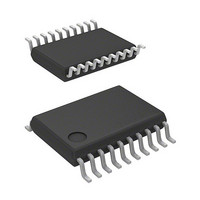
R5F21324ANSP#U1 Renesas Electronics America, R5F21324ANSP#U1 Datasheet - Page 495

R5F21324ANSP#U1
Manufacturer Part Number
R5F21324ANSP#U1
Description
MCU 1KB FLASH 16K ROM 20-LSSOP
Manufacturer
Renesas Electronics America
Series
R8C/3x/32Ar
Datasheet
1.R5F21322ANSPU1.pdf
(629 pages)
Specifications of R5F21324ANSP#U1
Core Processor
R8C
Core Size
16/32-Bit
Speed
20MHz
Connectivity
I²C, LIN, SIO, SSU, UART/USART
Peripherals
POR, PWM, Voltage Detect, WDT
Number Of I /o
15
Program Memory Size
16KB (16K x 8)
Program Memory Type
FLASH
Ram Size
1.5K x 8
Voltage - Supply (vcc/vdd)
1.8 V ~ 5.5 V
Data Converters
A/D 4x10b
Oscillator Type
Internal
Operating Temperature
-20°C ~ 85°C
Package / Case
20-LSSOP
Lead Free Status / RoHS Status
Lead free / RoHS Compliant
Eeprom Size
-
Available stocks
Company
Part Number
Manufacturer
Quantity
Price
- Current page: 495 of 629
- Download datasheet (7Mb)
Under development
R8C/32A Group
REJ09B0458-0020 Rev.0.20
Page 465 of 583
28. Comparator A
Comparator A compares a reference input voltage and an analog input voltage. Comparator A1 and comparator A2 are
independent of each other. Note that these comparators share the voltage detection circuit with voltage monitor 1 and
voltage monitor 2. Either comparator A1 and comparator A2 or voltage monitor 1 and voltage monitor 2 can be
selected to use the voltage detection circuit.
28.1
Table 28.1
Analog input voltage
Reference input voltage Input voltage to the LVREF pin
Comparison target
Comparison result
monitor
Interrupt
Digital
Filter
Comparison result
output
The comparison result of the reference input voltage and analog input voltage can be read by software. The result
also can be output from the VCOUTi (i = 1 or 2) pin. An input voltage to the LVREF pin can be selected as the
reference input voltage. Also, the comparator A1 interrupt and comparator A2 interrupt can be used.
Table 28.1 lists the Comparator A Specifications, Figure 28.1 shows a Comparator A Block Diagram, and Table
28.2 lists the Pin Configuration of Comparator A.
Overview
Switching
enable/disable
Sampling time
Item
Preliminary specification
Specifications in this manual are tentative and subject to change.
Comparator A Specifications
Input voltage to the LVCMP1 pin
Whether passing thorough the reference input voltage by rising or falling.
The VW1C3 bit in the VW1C register
Whether higher or lower than the reference input voltage.
Comparator A1 interrupt
(non-makable or maskable selectable)
Interrupt request at:
Reference input voltage >
input voltage to the LVCMP1 pin
and/or
Input voltage to the LVCMP1 pin >
reference input voltage
Supported
(fOCO-S divided by n) × 2
n: 1, 2, 4, and 8
Output from the LVCOUT1 pin
(Whether the comparison result output is
inverted or not can be selected.)
Nov 05, 2008
Comparator A1
Input voltage to the LVCMP2 pin
The VCA13 bit in the VCA1 register
Comparator A2 interrupt
(non-makable or maskable selectable)
Interrupt request at:
Reference input voltage >
input voltage to the LVCMP2 pin
and/or
Input voltage to the LVCMP2 pin >
reference input voltage
Output from the LVCOUT2 pin
(Whether the comparison result output is
inverted or not can be selected.)
Comparator A2
28. Comparator A
Related parts for R5F21324ANSP#U1
Image
Part Number
Description
Manufacturer
Datasheet
Request
R

Part Number:
Description:
KIT STARTER FOR M16C/29
Manufacturer:
Renesas Electronics America
Datasheet:

Part Number:
Description:
KIT STARTER FOR R8C/2D
Manufacturer:
Renesas Electronics America
Datasheet:

Part Number:
Description:
R0K33062P STARTER KIT
Manufacturer:
Renesas Electronics America
Datasheet:

Part Number:
Description:
KIT STARTER FOR R8C/23 E8A
Manufacturer:
Renesas Electronics America
Datasheet:

Part Number:
Description:
KIT STARTER FOR R8C/25
Manufacturer:
Renesas Electronics America
Datasheet:

Part Number:
Description:
KIT STARTER H8S2456 SHARPE DSPLY
Manufacturer:
Renesas Electronics America
Datasheet:

Part Number:
Description:
KIT STARTER FOR R8C38C
Manufacturer:
Renesas Electronics America
Datasheet:

Part Number:
Description:
KIT STARTER FOR R8C35C
Manufacturer:
Renesas Electronics America
Datasheet:

Part Number:
Description:
KIT STARTER FOR R8CL3AC+LCD APPS
Manufacturer:
Renesas Electronics America
Datasheet:

Part Number:
Description:
KIT STARTER FOR RX610
Manufacturer:
Renesas Electronics America
Datasheet:

Part Number:
Description:
KIT STARTER FOR R32C/118
Manufacturer:
Renesas Electronics America
Datasheet:

Part Number:
Description:
KIT DEV RSK-R8C/26-29
Manufacturer:
Renesas Electronics America
Datasheet:

Part Number:
Description:
KIT STARTER FOR SH7124
Manufacturer:
Renesas Electronics America
Datasheet:

Part Number:
Description:
KIT STARTER FOR H8SX/1622
Manufacturer:
Renesas Electronics America
Datasheet:

Part Number:
Description:
KIT DEV FOR SH7203
Manufacturer:
Renesas Electronics America
Datasheet:


