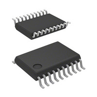
R5F21324ANSP#U1 Renesas Electronics America, R5F21324ANSP#U1 Datasheet - Page 119

R5F21324ANSP#U1
Manufacturer Part Number
R5F21324ANSP#U1
Description
MCU 1KB FLASH 16K ROM 20-LSSOP
Manufacturer
Renesas Electronics America
Series
R8C/3x/32Ar
Datasheet
1.R5F21322ANSPU1.pdf
(629 pages)
Specifications of R5F21324ANSP#U1
Core Processor
R8C
Core Size
16/32-Bit
Speed
20MHz
Connectivity
I²C, LIN, SIO, SSU, UART/USART
Peripherals
POR, PWM, Voltage Detect, WDT
Number Of I /o
15
Program Memory Size
16KB (16K x 8)
Program Memory Type
FLASH
Ram Size
1.5K x 8
Voltage - Supply (vcc/vdd)
1.8 V ~ 5.5 V
Data Converters
A/D 4x10b
Oscillator Type
Internal
Operating Temperature
-20°C ~ 85°C
Package / Case
20-LSSOP
Lead Free Status / RoHS Status
Lead free / RoHS Compliant
Eeprom Size
-
Available stocks
Company
Part Number
Manufacturer
Quantity
Price
- Current page: 119 of 629
- Download datasheet (7Mb)
Under development
R8C/32A Group
REJ09B0458-0020 Rev.0.20
Page 89 of 583
9.
The following five circuits are incorporated in the clock generation circuit:
• XIN clock oscillation circuit
• XCIN clock oscillation circuit
• Low-speed on-chip oscillator
• High-speed on-chip oscillator
• Low-speed on-chip oscillator for watchdog timer
9.1
Table 9.1
Notes:
Applications
Clock frequency 0 to 20 MHz
Connectable
oscillator
Oscillator
connect pins
Oscillation stop,
restart function
Oscillator status
after reset
Others
Table 9.1 lists the Specification Overview of Clock Generation Circuit. Figure 9.1 shows a Clock Generation
Circuit (With XIN and XCIN Pins Shared). Figure 9.2 shows a Peripheral Function Clock and Figure 9.3 shows a
Procedure for Reducing Internal Power Consumption Using VCA20 bit.
Clock Generation Circuit
1. These pins can be used as P4_6 or P4_7 when using the on-chip oscillator clock as the CPU clock while the
2. To input an external clock, set the CM05 bit in the CM0 register to 1 (XIN clock stops), the CM11 bit in the CM1
3. The clock frequency is automatically set to up to 20 MHz by a divider when using the high-speed on-chip
4. This applies when the CSPROINI bit in the OFS register is set to 1 (count source protection mode disabled after reset).
5. This applies when the CSPROINI bit in the OFS register is set to 0 (count source protection mode enabled after reset).
Item
XIN clock oscillation circuit and the XCIN clock oscillation circuit are not used.
register to 1 (internal feedback resistor disabled), and the CM13 bit to 1 (XIN-XOUT pin).
oscillator as the CPU clock source.
Overview
Specification Overview of Clock Generation Circuit
Preliminary specification
Specifications in this manual are tentative and subject to change.
Oscillation Circuit
• CPU clock
• Peripheral
• Ceramic
• Crystal
XIN, XOUT
Usable
Stop
Externally
generated clock
can be input
source
function clock
source
resonator
oscillator
XIN Clock
(1)
Nov 05, 2008
(2)
• CPU clock
• Peripheral
32.768 kHz
• Crystal
XCIN, XCOUT
Usable
Stop
• Externally
• On-chip
Oscillation Circuit
source
function clock
source
oscillator
generated clock
can be input
feedback
resistor Rf
(connected/
not connected
selectable)
XCIN Clock
(1)
On-Chip Oscillator
• CPU clock
• Peripheral
• CPU and
Approx. 40 MHz
−
−
Usable
Stop
−
source
function clock
source
peripheral
function clock
source when XIN
clock stops
oscillating
(1)
High-Speed
On-Chip Oscillator
(3)
• CPU clock
• Peripheral
• CPU and
Approx. 125 kHz
−
−
Usable
Oscillate
−
On-Chip Oscillator
source
function clock
source
peripheral
function clock
source when XIN
clock stops
oscillating
(1)
Low-Speed
9. Clock Generation Circuit
• Watchdog timer
Approx. 125 kHz
−
−
Usable
Stop
Oscillate
−
for Watchdog Timer
On-Chip Oscillator
clock source
Low-Speed
(4)
(5)
Related parts for R5F21324ANSP#U1
Image
Part Number
Description
Manufacturer
Datasheet
Request
R

Part Number:
Description:
KIT STARTER FOR M16C/29
Manufacturer:
Renesas Electronics America
Datasheet:

Part Number:
Description:
KIT STARTER FOR R8C/2D
Manufacturer:
Renesas Electronics America
Datasheet:

Part Number:
Description:
R0K33062P STARTER KIT
Manufacturer:
Renesas Electronics America
Datasheet:

Part Number:
Description:
KIT STARTER FOR R8C/23 E8A
Manufacturer:
Renesas Electronics America
Datasheet:

Part Number:
Description:
KIT STARTER FOR R8C/25
Manufacturer:
Renesas Electronics America
Datasheet:

Part Number:
Description:
KIT STARTER H8S2456 SHARPE DSPLY
Manufacturer:
Renesas Electronics America
Datasheet:

Part Number:
Description:
KIT STARTER FOR R8C38C
Manufacturer:
Renesas Electronics America
Datasheet:

Part Number:
Description:
KIT STARTER FOR R8C35C
Manufacturer:
Renesas Electronics America
Datasheet:

Part Number:
Description:
KIT STARTER FOR R8CL3AC+LCD APPS
Manufacturer:
Renesas Electronics America
Datasheet:

Part Number:
Description:
KIT STARTER FOR RX610
Manufacturer:
Renesas Electronics America
Datasheet:

Part Number:
Description:
KIT STARTER FOR R32C/118
Manufacturer:
Renesas Electronics America
Datasheet:

Part Number:
Description:
KIT DEV RSK-R8C/26-29
Manufacturer:
Renesas Electronics America
Datasheet:

Part Number:
Description:
KIT STARTER FOR SH7124
Manufacturer:
Renesas Electronics America
Datasheet:

Part Number:
Description:
KIT STARTER FOR H8SX/1622
Manufacturer:
Renesas Electronics America
Datasheet:

Part Number:
Description:
KIT DEV FOR SH7203
Manufacturer:
Renesas Electronics America
Datasheet:


