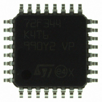
ST72F344K4T6 STMicroelectronics, ST72F344K4T6 Datasheet - Page 179

ST72F344K4T6
Manufacturer Part Number
ST72F344K4T6
Description
MCU 8BIT 16KB FLASH MEM 32-LQFP
Manufacturer
STMicroelectronics
Series
ST7r
Datasheet
1.ST72F344K2T6.pdf
(247 pages)
Specifications of ST72F344K4T6
Core Processor
ST7
Core Size
8-Bit
Speed
8MHz
Connectivity
I²C, LIN, SCI, SPI
Peripherals
LVD, POR, PWM, WDT
Number Of I /o
24
Program Memory Size
16KB (16K x 8)
Program Memory Type
FLASH
Eeprom Size
256 x 8
Ram Size
1K x 8
Voltage - Supply (vcc/vdd)
2.7 V ~ 5.5 V
Data Converters
A/D 12x10b
Oscillator Type
Internal
Operating Temperature
-40°C ~ 85°C
Package / Case
32-LQFP
Processor Series
ST72F3x
Core
ST7
Data Bus Width
8 bit
Data Ram Size
1 KB
Interface Type
I2C, SCI, SPI
Maximum Clock Frequency
8 MHz
Number Of Programmable I/os
34
Number Of Timers
2
Maximum Operating Temperature
+ 85 C
Mounting Style
SMD/SMT
Development Tools By Supplier
ST72F34X-SK/RAIS, ST7MDT40-EMU3, STX-RLINK
Minimum Operating Temperature
- 40 C
On-chip Adc
10 bit, 8 Channel
For Use With
497-5046 - KIT TOOL FOR ST7/UPSD/STR7 MCU
Lead Free Status / RoHS Status
Lead free / RoHS Compliant
Other names
497-5611
Available stocks
Company
Part Number
Manufacturer
Quantity
Price
Company:
Part Number:
ST72F344K4T6
Manufacturer:
STMicroelectronics
Quantity:
10 000
Company:
Part Number:
ST72F344K4T6TR
Manufacturer:
STMicroelectronics
Quantity:
10 000
- Current page: 179 of 247
- Download datasheet (3Mb)
ST72344xx ST72345xx
Note:
Note:
Bit 1= ITWE3 Interrupt enable on write to Slave 3
Bit 0 = ITWE1/2 Interrupt enable on write to Slave 1 or 2
I2C control register 2 (I2C3SCR2)
Reset value: 0000 0000 (00h)
Bits 7:5 = Reserved, must be kept at 0.
Bit 4 = WP2 Write Protect enable for Slave 2
Bit 3 = WP1 Write Protect enable for Slave 1
(Applicable for both WP2/ WP1)
Only write operations are disabled/enabled. Read operations are not affected.
If a write operation is attempted, the slave address is acknowledged, the current address
register is overwritten, data is also acknowledged but it is not written to the RAM.
Both the current address and byte count registers are incremented as in normal operation.
No interrupt generated if slave is write protected
BusyW will not be set if slave is write protected
Bit 2 = PE Peripheral enable
To enable the I
activates the interface (only PE is set)
This bit is set and cleared by software. It is also cleared by hardware when interface is
disabled.
0: Interrupt after write to Slave 3 disabled
1: Interrupt after write to Slave 3 enabled
This bit is set and cleared by software. It is also cleared by hardware when interface is
disabled software. It is also cleared by hardware when interface is disabled.
0: Interrupt after write to Slave 1 or 2 disabled
1: Interrupt after write to Slave 1 or 2 enabled
This bit is set and cleared by software. It is also cleared by hardware when the interface
is disabled (PE=0)
0: Write access to Slave 2 RAM buffer enabled
1: Write access to Slave 2 RAM buffer disabled
This bit is set and cleared by software. It is also cleared by hardware when the interface
is disabled (PE=0).
0: Write access to Slave 1 RAM buffer enabled
1: Write access to Slave 1 RAM buffer disabled
This bit is set and cleared by software.
0: Peripheral disabled
1: Slave capability enabled
7
0
2
C interface, write the CR register TWICE with PE=1 as the first write only
0
0
Doc ID 12321 Rev 5
WP2
Read / Write
WP1
PE
On-chip peripherals
BusyW
B/W
179/247
0
Related parts for ST72F344K4T6
Image
Part Number
Description
Manufacturer
Datasheet
Request
R

Part Number:
Description:
STMicroelectronics [RIPPLE-CARRY BINARY COUNTER/DIVIDERS]
Manufacturer:
STMicroelectronics
Datasheet:

Part Number:
Description:
STMicroelectronics [LIQUID-CRYSTAL DISPLAY DRIVERS]
Manufacturer:
STMicroelectronics
Datasheet:

Part Number:
Description:
BOARD EVAL FOR MEMS SENSORS
Manufacturer:
STMicroelectronics
Datasheet:

Part Number:
Description:
NPN TRANSISTOR POWER MODULE
Manufacturer:
STMicroelectronics
Datasheet:

Part Number:
Description:
TURBOSWITCH ULTRA-FAST HIGH VOLTAGE DIODE
Manufacturer:
STMicroelectronics
Datasheet:

Part Number:
Description:
Manufacturer:
STMicroelectronics
Datasheet:

Part Number:
Description:
DIODE / SCR MODULE
Manufacturer:
STMicroelectronics
Datasheet:

Part Number:
Description:
DIODE / SCR MODULE
Manufacturer:
STMicroelectronics
Datasheet:

Part Number:
Description:
Search -----> STE16N100
Manufacturer:
STMicroelectronics
Datasheet:

Part Number:
Description:
Search ---> STE53NA50
Manufacturer:
STMicroelectronics
Datasheet:

Part Number:
Description:
NPN Transistor Power Module
Manufacturer:
STMicroelectronics
Datasheet:

Part Number:
Description:
DIODE / SCR MODULE
Manufacturer:
STMicroelectronics
Datasheet:


