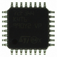
ST72F344K4T6 STMicroelectronics, ST72F344K4T6 Datasheet - Page 169

ST72F344K4T6
Manufacturer Part Number
ST72F344K4T6
Description
MCU 8BIT 16KB FLASH MEM 32-LQFP
Manufacturer
STMicroelectronics
Series
ST7r
Datasheet
1.ST72F344K2T6.pdf
(247 pages)
Specifications of ST72F344K4T6
Core Processor
ST7
Core Size
8-Bit
Speed
8MHz
Connectivity
I²C, LIN, SCI, SPI
Peripherals
LVD, POR, PWM, WDT
Number Of I /o
24
Program Memory Size
16KB (16K x 8)
Program Memory Type
FLASH
Eeprom Size
256 x 8
Ram Size
1K x 8
Voltage - Supply (vcc/vdd)
2.7 V ~ 5.5 V
Data Converters
A/D 12x10b
Oscillator Type
Internal
Operating Temperature
-40°C ~ 85°C
Package / Case
32-LQFP
Processor Series
ST72F3x
Core
ST7
Data Bus Width
8 bit
Data Ram Size
1 KB
Interface Type
I2C, SCI, SPI
Maximum Clock Frequency
8 MHz
Number Of Programmable I/os
34
Number Of Timers
2
Maximum Operating Temperature
+ 85 C
Mounting Style
SMD/SMT
Development Tools By Supplier
ST72F34X-SK/RAIS, ST7MDT40-EMU3, STX-RLINK
Minimum Operating Temperature
- 40 C
On-chip Adc
10 bit, 8 Channel
For Use With
497-5046 - KIT TOOL FOR ST7/UPSD/STR7 MCU
Lead Free Status / RoHS Status
Lead free / RoHS Compliant
Other names
497-5611
Available stocks
Company
Part Number
Manufacturer
Quantity
Price
Company:
Part Number:
ST72F344K4T6
Manufacturer:
STMicroelectronics
Quantity:
10 000
Company:
Part Number:
ST72F344K4T6TR
Manufacturer:
STMicroelectronics
Quantity:
10 000
- Current page: 169 of 247
- Download datasheet (3Mb)
ST72344xx ST72345xx
11.7.4
SDA/SCL line control
When the I2C3S interface is enabled, the SDA and SCL ports must be configured as floating
inputs. In this case, the value of the external pull-up resistor used depends on the
application.
When the I2C3S interface is disabled, the SDA and SCL ports revert to being standard I/O
port pins.
Figure 72. I
Functional description
The three slave addresses 1, 2 and 3 can be used as general purpose I
support all features of standard I
fully emulate them.
Slaves 1 and 2 are mapped on the same interrupt vector. Slave 3 has a separate interrupt
vector with higher priority.
The three slave addresses are defined by writing the 7 MSBs of the address in the
I2C3SSAR1, I2C3SSAR2 and I2C3SSAR3 registers. The slaves are enabled by setting the
enable bits in the same registers.
Each slave has its own RAM buffer at a fixed location in the ST7 RAM area.
●
●
All three slaves have individual read flags (RF) and write flags (WF) with maskable
interrupts. These flags are set when the I
Paged operation
To allow emulation of Standard I
buffer. The pages are configured using the PL[1:0] bits in the I2C3SCR1 register. 8/16-Byte
page length has to be selected depending on the EEPROM device to emulate. The Full
Page option is to be used when no paging of the RAM buffer is required. The configuration is
common to the 3 slave addresses. The Full Page configuration corresponds to 256 bytes for
address 1 and 2 and to 128 bytes for address 3.
Paging affects the handling of rollover when write operations are performed. In case the
bottom of the page is reached, the write continues from the first address of the same page.
Page length does not affect read operations: rollover is done on the whole RAM buffer
whatever the configured page length.
Slaves 1 and 2 have 256-byte buffers which can be individually protected from I
master write accesses.
Slave 3 has a 128-byte RAM buffer without write protection feature.
2
C bus protocol
SCL
SDA
condition
Start
Doc ID 12321 Rev 5
MSB
2
1
2
C EEPROM devices, pages can be defined in the RAM
C EEPROMs like the ST M24Cxx family and are able to
2
2
C master has completed a read or write operation.
8
ACK
9
condition
On-chip peripherals
2
Stop
C slaves. They also
2
169/247
C
Related parts for ST72F344K4T6
Image
Part Number
Description
Manufacturer
Datasheet
Request
R

Part Number:
Description:
STMicroelectronics [RIPPLE-CARRY BINARY COUNTER/DIVIDERS]
Manufacturer:
STMicroelectronics
Datasheet:

Part Number:
Description:
STMicroelectronics [LIQUID-CRYSTAL DISPLAY DRIVERS]
Manufacturer:
STMicroelectronics
Datasheet:

Part Number:
Description:
BOARD EVAL FOR MEMS SENSORS
Manufacturer:
STMicroelectronics
Datasheet:

Part Number:
Description:
NPN TRANSISTOR POWER MODULE
Manufacturer:
STMicroelectronics
Datasheet:

Part Number:
Description:
TURBOSWITCH ULTRA-FAST HIGH VOLTAGE DIODE
Manufacturer:
STMicroelectronics
Datasheet:

Part Number:
Description:
Manufacturer:
STMicroelectronics
Datasheet:

Part Number:
Description:
DIODE / SCR MODULE
Manufacturer:
STMicroelectronics
Datasheet:

Part Number:
Description:
DIODE / SCR MODULE
Manufacturer:
STMicroelectronics
Datasheet:

Part Number:
Description:
Search -----> STE16N100
Manufacturer:
STMicroelectronics
Datasheet:

Part Number:
Description:
Search ---> STE53NA50
Manufacturer:
STMicroelectronics
Datasheet:

Part Number:
Description:
NPN Transistor Power Module
Manufacturer:
STMicroelectronics
Datasheet:

Part Number:
Description:
DIODE / SCR MODULE
Manufacturer:
STMicroelectronics
Datasheet:


