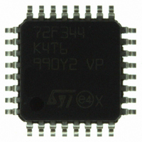
ST72F344K4T6 STMicroelectronics, ST72F344K4T6 Datasheet - Page 146

ST72F344K4T6
Manufacturer Part Number
ST72F344K4T6
Description
MCU 8BIT 16KB FLASH MEM 32-LQFP
Manufacturer
STMicroelectronics
Series
ST7r
Datasheet
1.ST72F344K2T6.pdf
(247 pages)
Specifications of ST72F344K4T6
Core Processor
ST7
Core Size
8-Bit
Speed
8MHz
Connectivity
I²C, LIN, SCI, SPI
Peripherals
LVD, POR, PWM, WDT
Number Of I /o
24
Program Memory Size
16KB (16K x 8)
Program Memory Type
FLASH
Eeprom Size
256 x 8
Ram Size
1K x 8
Voltage - Supply (vcc/vdd)
2.7 V ~ 5.5 V
Data Converters
A/D 12x10b
Oscillator Type
Internal
Operating Temperature
-40°C ~ 85°C
Package / Case
32-LQFP
Processor Series
ST72F3x
Core
ST7
Data Bus Width
8 bit
Data Ram Size
1 KB
Interface Type
I2C, SCI, SPI
Maximum Clock Frequency
8 MHz
Number Of Programmable I/os
34
Number Of Timers
2
Maximum Operating Temperature
+ 85 C
Mounting Style
SMD/SMT
Development Tools By Supplier
ST72F34X-SK/RAIS, ST7MDT40-EMU3, STX-RLINK
Minimum Operating Temperature
- 40 C
On-chip Adc
10 bit, 8 Channel
For Use With
497-5046 - KIT TOOL FOR ST7/UPSD/STR7 MCU
Lead Free Status / RoHS Status
Lead free / RoHS Compliant
Other names
497-5611
Available stocks
Company
Part Number
Manufacturer
Quantity
Price
Company:
Part Number:
ST72F344K4T6
Manufacturer:
STMicroelectronics
Quantity:
10 000
Company:
Part Number:
ST72F344K4T6TR
Manufacturer:
STMicroelectronics
Quantity:
10 000
- Current page: 146 of 247
- Download datasheet (3Mb)
On-chip peripherals
Note:
Note:
146/247
Bit 1 = RWU Receiver wake-up.
Before selecting Mute mode (by setting the RWU bit) the SCI must first receive a data byte,
otherwise it cannot function in Mute mode with wake-up by Idle line detection.
In Address Mark Detection Wake-Up configuration (WAKE bit = 1) the RWU bit cannot be
modified by software while the RDRF bit is set.
Bit 0 = SBK Send break.
If the SBK bit is set to “1” and then to “0”, the transmitter sends a BREAK word at the end of
the current word.
Data register (SCIDR)
Reset value: Undefined
Contains the Received or Transmitted data character, depending on whether it is read from
or written to.
The Data register performs a double function (read and write) since it is composed of two
registers, one for transmission (TDR) and one for reception (RDR).
The TDR register provides the parallel interface between the internal bus and the output
shift register (see
The RDR register provides the parallel interface between the input shift register and the
internal bus (see
Baud rate register (SCIBRR)
Reset value: 0000 0000 (00h)
Bits 7:6 = SCP[1:0] First SCI Prescaler
These 2 prescaling bits allow several standard clock division ranges as shown in
SCP1
DR7
This bit determines if the SCI is in mute mode or not. It is set and cleared by software
and can be cleared by hardware when a wake-up sequence is recognized.
0: Receiver in active mode
1: Receiver in mute mode
This bit set is used to send break characters. It is set and cleared by software.
0: No break character is transmitted
1: Break characters are transmitted
7
7
SCP0
DR6
Figure
Figure
63).
63).
SCT2
DR5
Doc ID 12321 Rev 5
SCT1
DR4
Read/Write
Read/Write
SCT0
DR3
SCR2
DR2
ST72344xx ST72345xx
SCR1
DR1
Figure
SCR0
DR0
0
0
59.
Related parts for ST72F344K4T6
Image
Part Number
Description
Manufacturer
Datasheet
Request
R

Part Number:
Description:
STMicroelectronics [RIPPLE-CARRY BINARY COUNTER/DIVIDERS]
Manufacturer:
STMicroelectronics
Datasheet:

Part Number:
Description:
STMicroelectronics [LIQUID-CRYSTAL DISPLAY DRIVERS]
Manufacturer:
STMicroelectronics
Datasheet:

Part Number:
Description:
BOARD EVAL FOR MEMS SENSORS
Manufacturer:
STMicroelectronics
Datasheet:

Part Number:
Description:
NPN TRANSISTOR POWER MODULE
Manufacturer:
STMicroelectronics
Datasheet:

Part Number:
Description:
TURBOSWITCH ULTRA-FAST HIGH VOLTAGE DIODE
Manufacturer:
STMicroelectronics
Datasheet:

Part Number:
Description:
Manufacturer:
STMicroelectronics
Datasheet:

Part Number:
Description:
DIODE / SCR MODULE
Manufacturer:
STMicroelectronics
Datasheet:

Part Number:
Description:
DIODE / SCR MODULE
Manufacturer:
STMicroelectronics
Datasheet:

Part Number:
Description:
Search -----> STE16N100
Manufacturer:
STMicroelectronics
Datasheet:

Part Number:
Description:
Search ---> STE53NA50
Manufacturer:
STMicroelectronics
Datasheet:

Part Number:
Description:
NPN Transistor Power Module
Manufacturer:
STMicroelectronics
Datasheet:

Part Number:
Description:
DIODE / SCR MODULE
Manufacturer:
STMicroelectronics
Datasheet:


